Direct graphene film transfer method

A graphene film, a direct technology, applied in the field of nanomaterials, can solve the problems of inconvenient transfer of graphene film, slow pace of practical application of graphene, etc., and achieve the effect of easy industrial application, controllable product size and simple equipment

Inactive Publication Date: 2012-08-01
ZHEJIANG UNIV
View PDF2 Cites 39 Cited by
  • Summary
  • Abstract
  • Description
  • Claims
  • Application Information

AI Technical Summary

Problems solved by technology

At present, the large-area graphene film is mainly prepared by chemical vapor deposition. This method mainly uses the metal surface to deposit carbon atoms to generate graphene. It is very inconvenient to transfer graphene film from the metal surface, which has caused the pace of industrialization and practicalization of graphene. slow

Method used


Image

  • Direct graphene film transfer method
  • Direct graphene film transfer method
  • Direct graphene film transfer method

Examples


Embodiment 1

[0021] Example 1: The graphene film on the copper foil is transferred to a circular hole carrier screen.

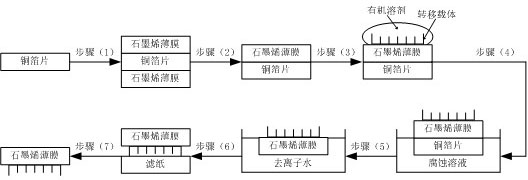
[0022] Such as figure 1 As shown in the flow chart, firstly, a graphene film is grown on a 25-micron thick copper foil using a CVD device; then an oxygen plasma cleaner is used to clean the graphene on one side of the copper foil. The cleaning voltage is 650V and the cleaning time is 3 minutes. , To obtain a combination of a single-layer graphene film and a copper foil; then flatly affix the circular hole carrier net on the single-layer graphene film, and add 5 mL isopropanol to the edge of the carrier net to make the carrier net and the graphene film fully contact , The aperture of the carrier net is 1 micron; then the combination of the round hole carrier net, graphene film and copper foil is immersed in a ferric chloride aqueous solution with a molar mass of 0.5 mol / L, and the copper foil is completely corroded after 40 minutes; The combination of the round hole carrier n...

Embodiment 2

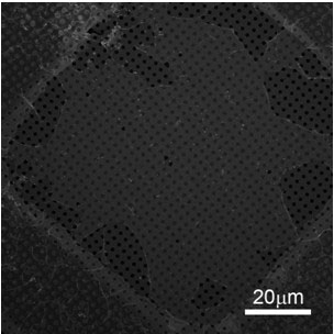
[0023] Example 2: Transfer the graphene film on the copper foil to the elliptical carrier net.

[0024] The specific steps are similar to those in Example 1, but the transfer carrier is an elliptical carrier net, and the scanned image is as Figure 5 As shown, the size of the complete graphene film reaches about 100 microns.

Embodiment 3

[0025] Example 3: Transfer the graphene film on the copper foil to the silica substrate.

[0026] The specific steps are similar to Example 1, but the transfer carrier is a silica substrate. In step 4, the silica substrate needs to be suspended and fixed so that the combination of the silica substrate, graphene film and copper foil is tightly attached to the surface of the etching solution .


PUM


Abstract

The invention relates to a direct graphene film transfer method. Currently, transferring graphene films from metal surfaces is quite inconvenient. The method includes: using the chemical vapor deposition method to grow a graphene film on a copper foil; using oxygen plasma cleaner to clear graphene on one side of the copper foil to obtain a combination of the single-layer graphene film with the copper foil; flatly attaching a transfer carrier onto the surface of the graphene film and drip adding an organic solvent of a proper quality to increase the interaction between the transfer carrier andthe graphene film; using etchant solution to clear the copper foil to obtain a combination of the single-layer graphene film with the transfer carrier; using deionized water to clean the graphene film for multiple times; and using a filter paper to clear the deionized water on the surface of the graphene film. Using the direct graphene film transfer method avoids the graphene films from being damaged by transfer media such as organic colloid and the like, single-layer graphene films of 100 micrometers or more can be obtained, simple equipment is required, product dimension is controllable, production safety is high, and industrial application is easy to implement.

Description

Technical field [0001] The invention relates to the field of nanomaterials, and relates to a method for directly transferring graphene films. Background technique [0002] Graphene is sp 2 Hexagonal honeycomb-shaped planar body with a single layer of atoms arranged by hybrid carbon atoms. Graphene is the thinnest and hardest material known in the universe. The carriers in it show a huge mobility, and the effective mass of the carriers is zero. It can pass through micron-level matter at room temperature without scattering. The maximum current density that graphene can carry is six orders of magnitude higher than that of copper, and it has high thermal conductivity and high mechanical strength. Graphene is widely believed to eventually replace silicon materials, triggering a revolution in the electronics industry. Following the discovery of fullerenes and carbon nanotubes, the emergence of graphene and the prospects for industrialized applications have made carbon nanotechnology...

Claims


Application Information

Patent Timeline
Patent Type & Authority Applications(China)
IPC IPC(8): C01B31/04C01B32/186C01B32/194
Inventor 董策舟王宏涛聂安民周武李倩倩
Owner ZHEJIANG UNIV
Why Eureka
Try Eureka