Thiol-ene based poly(alkylsiloxane) materials

a technology of alkylsiloxane and thiol-ene, which is applied in the field of patterned thiolene polymers, can solve the problems of limited number of reliable materials for soft lithography or imprints, low ym value, and brittleness of materials, etc., and achieves low ym value, easy to make, and easy to tune the physical properties of stamps.

Inactive Publication Date: 2009-04-16
RGT UNIV OF CALIFORNIA
View PDF4 Cites 37 Cited by
  • Summary
  • Abstract
  • Description
  • Claims
  • Application Information

AI Technical Summary

Benefits of technology

[0010]Currently, there are a limited number of reliable materials for soft lithography or imprint lithography. In general, these materials tend to be either brittle, difficult to make, and / or have very low YM values (1-10 MPa), among other important factors. Thiol-ene photo-polymerizations1 offer a viable means to use readily available and inexpensive materials, by means of simplistic photochemical cross-linking conditions without the rigorous exclusion of oxygen. The reaction involves the use of compounds with thiols and alkene groups, in the presence of a small amount of a radical photoinitiator, to carry out the cross-linking via radical addition to double bonds and radical-radical recombinations. By appropriately screening the monomer materials, tuning of the physical properties of the stamps should be readily accomplished. Similarly, the manipulation to apply the materials to variable conditions can be easily adjusted by understanding and controlling the effect of the monomer units on the bulk properties. The present invention has discovered that thiolpropyl substituted poly(mercaptopropylmethylsiloxane) (PMMS), is the optimum material for imprint lithography and leads to a variety of composition of matter claims when blended with a series of alkene-functional monomers. The performance of these materials far exceeds current formulations disclosed in the literature and is non-obvious, and the choice of PMMS is critical as it gives a solid patent position for both materials as well as process filings.
[0014]The physical properties are typically controlled by one or more of the following: a composition of the alkene monomers, an alkene monomer to thiol weight to weight ratio (ene:thiol ratio), a structure of the alkene monomers and physical properties of the alkene functional monomers. For example, the physical properties may enable the thiol-ene polymer to be molded into submicron and nano scale features with aspect ratios of up to 5 without collapse of the features. Several different alkene monomers may be blended with the thiol compound, for example, a first composition of one of the alkene monomers may allow the thiol-ene polymer to withstand a stress greater than 1 MPa and a second composition of one of the alkene monomers may allow the thiol-ene polymer to have a strain percentage between 5% and 55%. Specifically, the alkene monomers may comprise BPADMA to increase a stress the thiolene polymer can withstand without breaking, as compared to without the BPADMA, and may further comprise EGDA to increase a flexibility of the thiol-ene polymer as compared to without the EGDA. The alkene monomers may further comprise TAOTA to render the poly thiol compound PMMS and BPADMA miscible.

Problems solved by technology

Currently, there are a limited number of reliable materials for soft lithography or imprint lithography.
In general, these materials tend to be either brittle, difficult to make, and / or have very low YM values (1-10 MPa), among other important factors.

Method used


Image

  • Thiol-ene based poly(alkylsiloxane) materials
  • Thiol-ene based poly(alkylsiloxane) materials
  • Thiol-ene based poly(alkylsiloxane) materials

Examples


Embodiment Construction

[0036]In the following description of the preferred embodiment, reference is made to the accompanying drawings which form a part hereof, and in which is shown by way of illustration a specific embodiment in which the invention may be practiced. It is to be understood that other embodiments may be utilized and structural changes may be made without departing from the scope of the present invention.

[0037]Technical Description

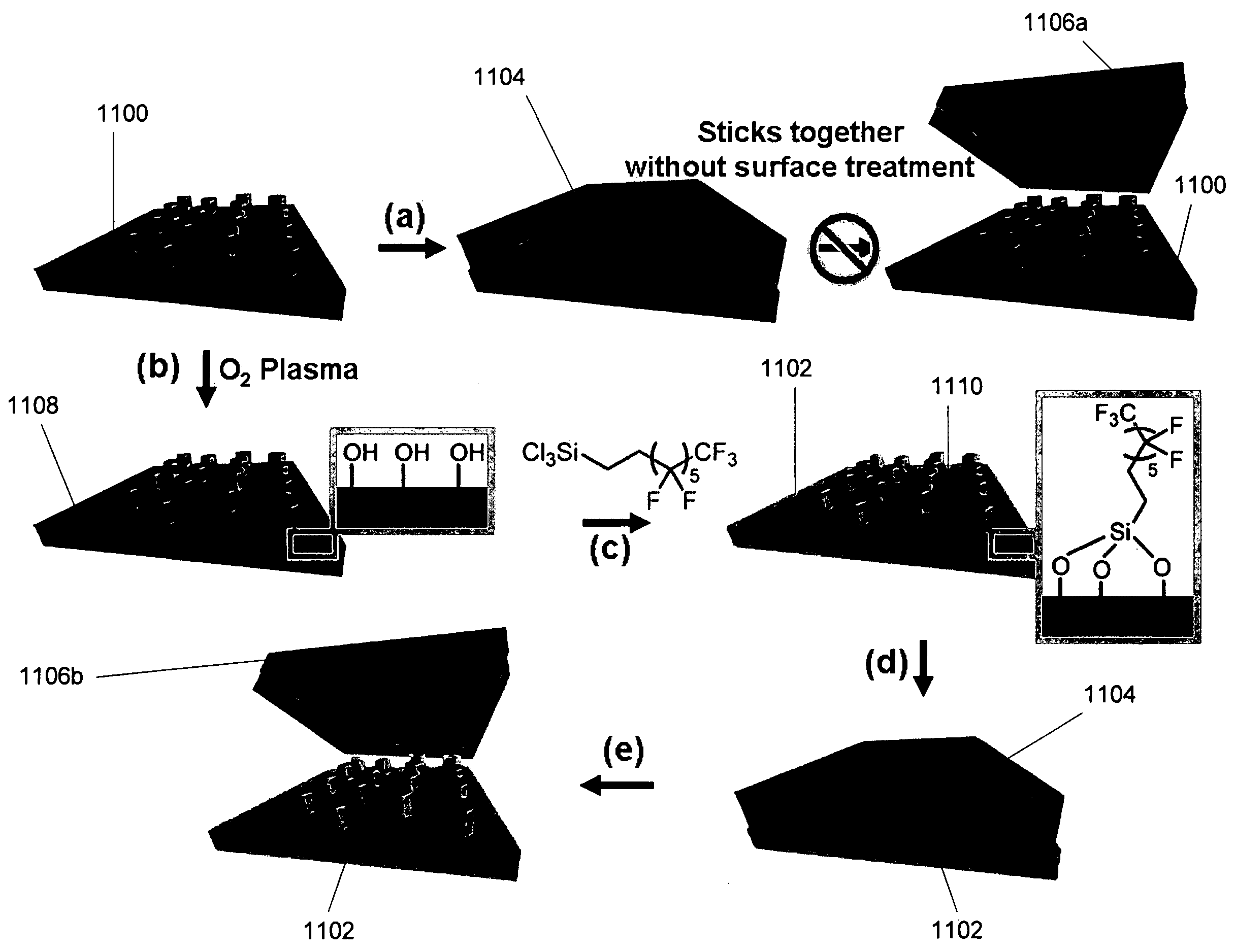
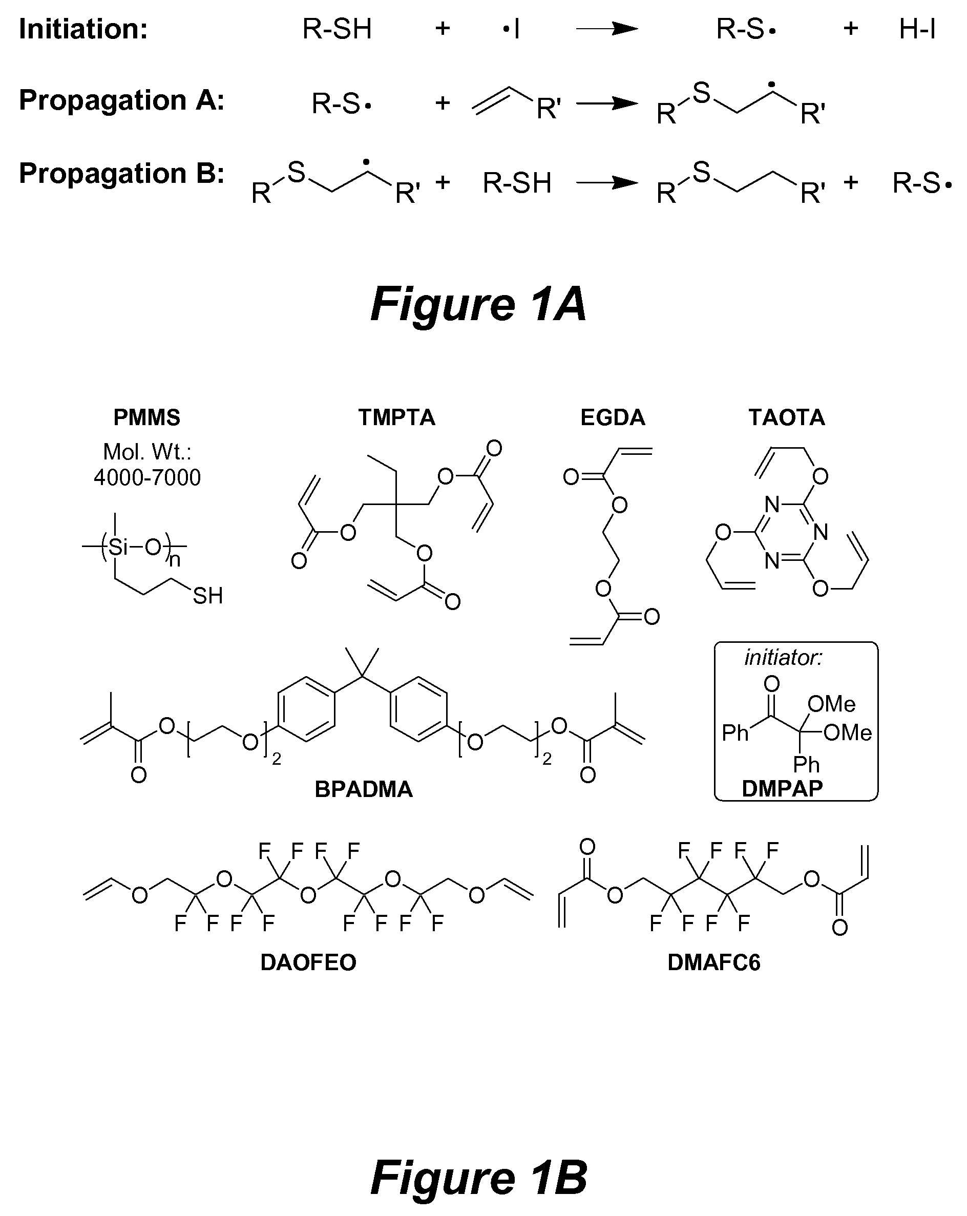
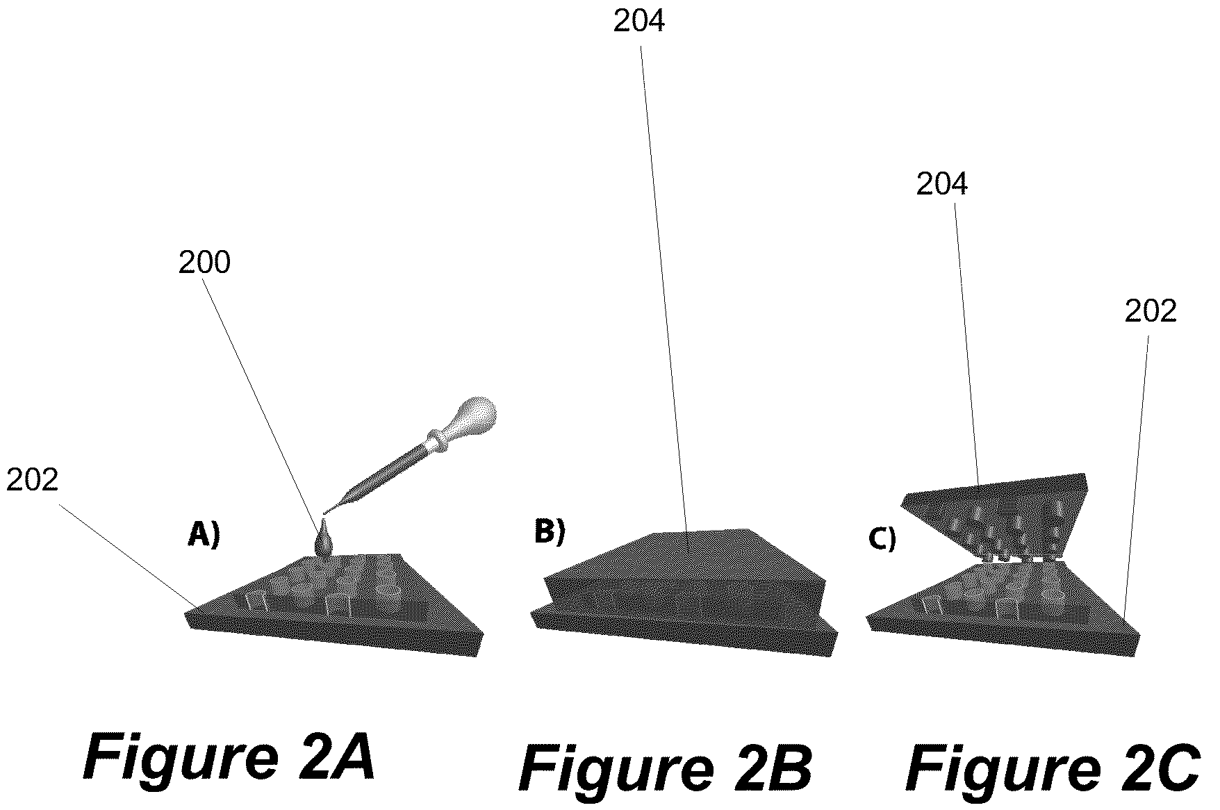
[0038]In a radical approach, the present invention seeks to optimize not only the physical properties of PDMS-based stamp materials, but also the process by which they are made. It is of utmost importance to develop materials that can be easily blended to yield high fidelity composites in a fast and reliable fashion with viable means of tuning their bulk properties. Thus, the present invention allows the user to manufacture multiple stamps in a short period of time (within minutes), for parallel printing over large areas, and at very low cost. In this regard, thio...


PUM

PropertyMeasurementUnit
temperaturesaaaaaaaaaa
wavelengthsaaaaaaaaaa
aspect ratiosaaaaaaaaaa

Abstract

A stamp is comprised of a thiol-ene polymer, wherein the thiol-ene polymer allows for creation of micro-scale or nano-scale patterns useful in soft or imprint lithography. A patterned thiol-ene polymer is fabricated by casting a thiol-ene mixture onto a patterned mold, curing the thiol-ene mixture to form the patterned thiol-ene polymer, and peeling off the patterned thiol-ene polymer from the silicon mold. A stamp comprised of a thiol-ene polymer may be replicated by exposing the to oxygen plasma to form a hydrophilic mold, exposing the hydrophilic mold to a fluorinating agent under vacuum conditions to form a functionalized surface of the hydrophilic mold, casting a thiol-ene mixture on top of the functionalized surface, photocuring the thiolene mixture to form a replica thiol-ene polymer, and peeling off the replica thiol-ene polymer.

Description

CROSS REFERENCE TO RELATED APPLICATIONS[0001]This application claims the benefit under 35 U.S.C. Section 119(e) of co-pending and commonly-assigned U.S. Provisional Patent Application Ser. No. 60 / 979,767, filed on Oct. 12, 2007, Craig J. Hawker, Luis M. Campos and Ines Meinel, entitled “THIOL-ENE BASED POLY(ALKYLSILOXANE) MATERIALS” attorneys' docket number 30794.251-US-P1 (2008-055-1), which application is incorporated by reference herein.[0002]This application is related to the following co-pending and commonly-assigned U.S. patent applications:[0003]U.S. Utility application Ser. No. ______, filed on same date herewith, by Craig J. Hawker, Luis M. Campos and Ines Meinel, entitled “METHOD FOR NON-DESTRUCTIVE PATTERNING OF PHOTONIC CRYSTALS EMPLOYED FOR SOLID-STATE LIGHT EXTRACTION,” attorney's docket number 30794.252-US-U1 (2008-054), which application claims the benefit under 35 U.S.C. Section 119(e) of co-pending and commonly-assigned U.S. Provisional Patent Application Ser. No. ...

Claims


Application Information

Patent Timeline
Patent Type & Authority Applications(United States)
IPC IPC(8): B29C59/14C08G75/04C08G77/04C08G63/06B28B11/08C08G63/195C08F2/46
CPCC08F2/48C08L83/08C08L81/02C08G75/045C08G75/12
Inventor HAWKER, CRAIG J.CAMPOS, LUIS M.MEINEL, INES
Owner RGT UNIV OF CALIFORNIA
Why Eureka
Try Eureka