Semiconductor device and manufacturing method thereof

a technology of semiconductor devices and manufacturing methods, applied in the direction of semiconductor devices, electrical devices, transistors, etc., can solve the problems of impracticality, damage to the insulating film residing below the tin film, and the technique of patent document 1 is hardly practical, so as to achieve the effect of practical level of work function differen

Inactive Publication Date: 2007-08-16
TOKYO ELECTRON LTD
View PDF4 Cites 11 Cited by
  • Summary
  • Abstract
  • Description
  • Claims
  • Application Information

AI Technical Summary

Benefits of technology

[0007]It is, therefore, an object of the present invention to provide a CMISFET semiconductor device and a manufacturing method therefor, capable of achieving a practical level of a work function difference between gate electrodes of two conductive regions without causing damages on an underlying gate insulating film.

Problems solved by technology

However, in the technique disclosed in Article 1, since the TiN film formed in the n-type MISFET region needs to be removed during the manufacturing process, a gate insulating film residing below the TiN film may be subject to damage.
Further, in Article 2, an HfSiON film is used as a gate insulating film, and a flat band voltage difference (relating to a work function difference) between the n-type MISFET having the NiSi metal gate electrode and the p-type MISFET having the Ni3Si metal gate electrode is as small as 0.25 V, thereby making the technique impractical.
However, upon reviewing by the inventors of the present invention, the technique of Patent Document 1 proves to be hardly a practical one.
As a result, the gate electrodes experience relatively high temperatures, which reduces the work function difference between the gate electrodes.
As discussed above, despite the demand to obtain a technique capable of achieving a practical level of a work function difference between gate electrodes of an n-type and a p-type MISFET region without causing damages on an underlying gate insulating film, no such technique has been realized.

Method used


Image

  • Semiconductor device and manufacturing method thereof
  • Semiconductor device and manufacturing method thereof
  • Semiconductor device and manufacturing method thereof

Examples


first embodiment

[0047]A first embodiment of the present invention will be described, first.

[0048]FIGS. 1 to 11 show cross sectional views to explain a series of processes of a method in accordance with the first embodiment of the present invention.

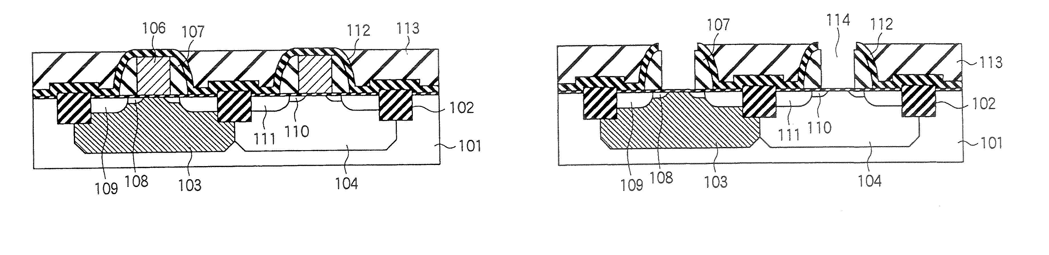
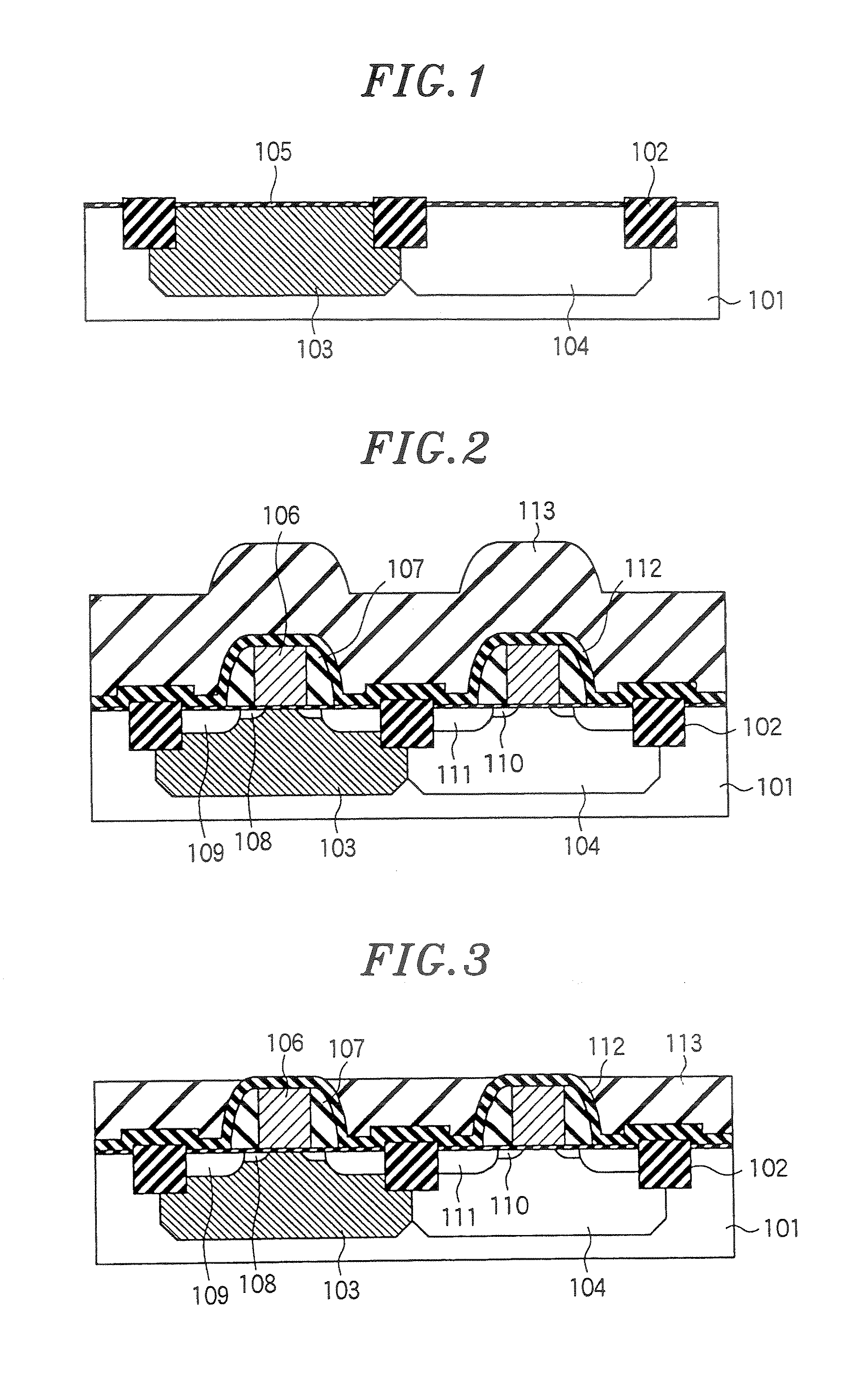
[0049]First, device isolation regions 102, a p-type well 103 that will be an n-type MISFET region, an n-type well 104 that will be a p-type MISFET region and a silicon oxide film 105 are formed at the surface region of a semiconductor substrate 101 mainly formed of silicon, as illustrated in FIG. 1.

[0050]Next, as shown in FIG. 2, dummy gate electrodes 106 made of polycrystalline silicon or the like, gate sidewalls 107 made of an insulating film such as a silicon nitride film or the like, extensions 108 of the n-type MISFET, a source / drain regions 109 of the n-type MISFET, extensions 110 of the p-type MISFET, source / drain regions 111 of the p-type MISFET, a silicon nitride film 112 serving as a contact etching stopper and an interlayer insulating film 113 ...

second embodiment

[0064]Hereinafter, a second embodiment of the present invention will be described.

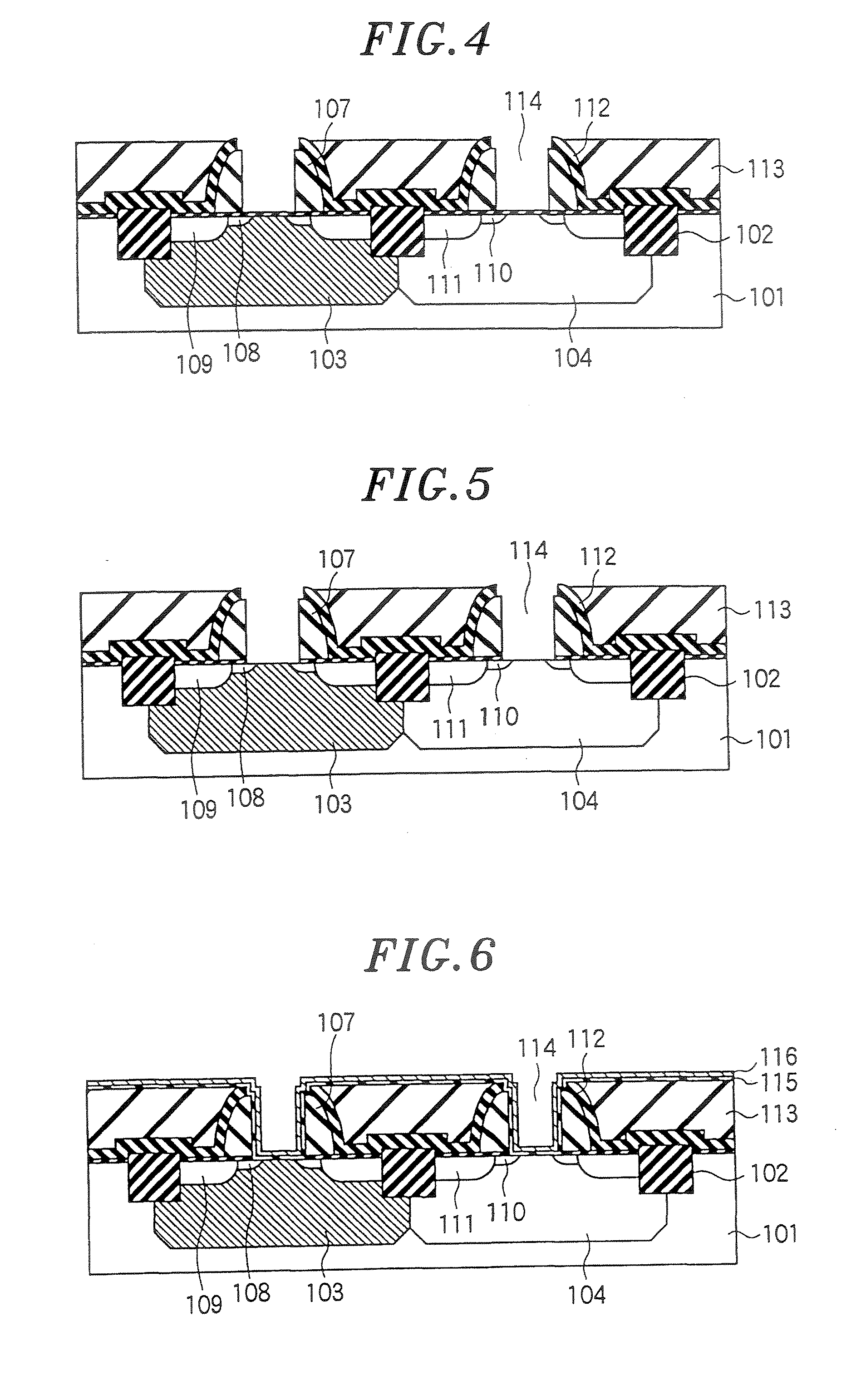
[0065]FIGS. 13 to 17 present cross sectional views to explain a series of processes of a method in accordance with the second embodiment of the present invention. In this embodiment, the processes illustrated in FIGS. 1 to 6 of the first embodiment are equally performed first. As for the gate insulating film 115 and the metal gate electrode material film 116, the same films used in the first embodiment may be employed. Next, a silicon film 119′ is deposited on the metal gate electrode material film 116, as shown in FIG. 13. In this case, the silicon film 119′ is deposited by using a film forming method enabling a low temperature deposition, e.g., a sputtering method or the like, to thereby prevent the silicide from being formed in the p-type MISFET region.

[0066]Next, as illustrated in FIG. 14, an etching mask 124 such as a photoresist or the like is formed on the n-type MISFET region and, then, the sil...

third embodiment

[0071]Hereinafter, a third embodiment of the present invention will be described.

[0072]FIGS. 18 to 23 represent cross sectional views to explain a method in accordance with the third embodiment of the present invention. In this embodiment, the processes illustrated in FIGS. 1 to 6 of the first embodiment are equally performed. As for the gate insulating film 115 and the metal gate electrode material film 116, the same films used in the first embodiment may be used. Thereafter, the processes described in FIGS. 13 to 15 of the second embodiment are equally performed.

[0073]Thereafter, by performing the heat treatment, only the metal gate electrode material film 116 of the n-type MISFET region reacts with the silicon film 119′, and an alloy forming reaction (silicide forming reaction) takes place, which generates a silicide film 120, as shown in FIG. 18.

[0074]Next, a germanium film 125 is formed on an entire surface as depicted in FIG. 19. Thereafter, an etching mask 126 such as a photo...


PUM


Abstract

In a method for manufacturing a semiconductor device, an insulating film is formed on an entire surface of a substrate having a device isolation region and a first and a second conductive region. Then, a semiconductor device structure having a gate electrode forming region is formed on each of the conductive regions, the insulating film being disposed between the gate electrode forming region and each of the conductive regions. A gate electrode groove is formed in the gate electrode forming region of the semiconductor device structure, the insulating film being removed in the gate electrode groove. Thereafter, a gate insulating film and a film of metal gate electrode material are deposited on a bottom surface and a side surface of the gate electrode groove and an alloy is formed by alloying the film of metal gate electrode material deposited in a gate electrode groove of the first conductive region.

Description

FIELD OF THE INVENTION[0001]The present invention relates to a semiconductor device; and, more particularly, to a CMISFET (Complementary Metal Insulator Semiconductor Field Effect Transistor) having an n-type and a p-type MISFET region, each having a metal gate electrode, and a manufacturing method thereof.BACKGROUND OF THE INVENTION[0002]Recently, a high-performance CMISFET, which includes an n-type and a p-type MISFET metal gate electrode having different work functions, has been gaining attention. For example, Article 1 (Samavedam et al., IDEM Tech. Dig., (2002) p. 443) discloses a technique of manufacturing a CMISFET, wherein by forming a TiN film for the p-type MISFET electrode throughout the entire surface of a wafer; removing the TiN film from the n-type MISFET region; and then depositing a TaSiN and a poly silicon film, the CMISFET is made to include a p-type MISFET region having a TiN electrode and an n-type MISFET region having a TaSiN electrode. Moreover, Article 2 (Terai...

Claims


Application Information

Patent Timeline
Patent Type & Authority Applications(United States)
IPC IPC(8): H01L21/4763H01L21/3205
CPCH01L21/823835H01L21/823842H01L29/4966H01L29/7833H01L29/66545H01L29/6659H01L29/517H01L21/28518
Inventor NAKAMURA, GENJIAKASAKA, YASUSHI
Owner TOKYO ELECTRON LTD
Why Eureka
Try Eureka