Unlock instant, AI-driven research and patent intelligence for your innovation.

Organic thin film transistor comprising fluorine-based polymer thin film and method for fabricating the same

a fluorine-based polymer and organic technology, applied in the field of organic thin film transistors, can solve the problems of unsatisfactory charge mobility, decreased charge mobility and increased reduced charge mobility and increase operating voltage and threshold voltage, so as to improve the ion/ion ratio, reduce the contact resistance between and between

Active Publication Date: 2007-08-23
SAMSUNG ELECTRONICS CO LTD
View PDF10 Cites 12 Cited by
  • Summary
  • Abstract
  • Description
  • Claims
  • Application Information

AI Technical Summary

Benefits of technology

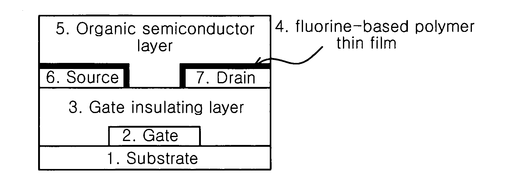
[0016]Example embodiments provide OTFTs using polymer semiconductors able to be subjected to a wet process with a fluorine-based polymer that material may be applied between source / drain electrodes and an organic semiconductor layer to form a fluorine-based polymer thin film, thereby decreasing the contact resistance therebetween, leading to improved charge mobility and Ion / Ioff ratio.

Problems solved by technology

However, the OTFT is disadvantageous because it has decreased charge mobility and increased operating voltage and threshold voltage compared with amorphous silicon TFTS.
However, charge mobility may still be unsatisfactory, and an operating voltage of about 100 V or more and a sub-threshold voltage corresponding to at least 50 times the voltage of an amorphous silicon TFT may be required.
Although the operating voltage of the OTFT is decreased to about −5 V, charge mobility thereof may not be higher than about 0.6 cm2·V−1·sec−1, which is still unsatisfactory.
A general wet process, e.g., simple coating and / or printing, may be difficult to use upon the fabrication of the device.
However, the organic insulating film may not exhibit the device properties suitable for substituting for an inorganic insulating film.
However, the above-mentioned are limited only to inorganic TFTs using amorphous silicon or monocrystal silicon, and may be more difficult to apply to organic semiconductors due to the use of inorganic material.
Accordingly, research into methods of forming an organic gate insulating layer through a simpler process and of increasing charge mobility between the organic gate insulating layer and the organic semiconductor layer thereon has been actively conducted, but there are no satisfactory alternatives.
However, among these structures, a top contact type OTFT may be undesirable because channel resistance is problematic.
A bottom contact type or top gate type OTFT may be undesirable because it has increased contact resistance between source / drain electrodes and an organic semiconductor layer, in addition to the problem of the channel resistance, undesirably deteriorating the performance of the OTFT.

Method used


Image

  • Organic thin film transistor comprising fluorine-based polymer thin film and method for fabricating the same
  • Organic thin film transistor comprising fluorine-based polymer thin film and method for fabricating the same
  • Organic thin film transistor comprising fluorine-based polymer thin film and method for fabricating the same

Examples


example 1

[0069]On a glass substrate having an Al gate electrode formed thereon, an organic insulator composition including a blend of a polyvinylphenyl copolymer and an acrylic crosslinking agent was applied through spin coating to form an insulating layer having a thickness of about 7000 Å, which was then subjected to baking at about 100° C. for about 1 hour in a nitrogen atmosphere, thus forming a gate insulating layer having a final thickness of about 6000 Å.

[0070]Gold (Au) source / drain electrodes were formed on the gate insulating layer through a bottom contact process using a shadow mask having a channel length of about 100 μm and a channel width of about 1 mm. Thereafter, the composition of Preparative Example 1 was dissolved to about 0.5 wt % in cyclohexanone, and the solution thus obtained was then applied on the source / drain electrodes through spin coating at about 3000 rpm, to form a fluorine-based polymer thin film about 80 Å thick, which was then cured at about 150° C. for about ...

example 2

[0080]An OTFT was fabricated in the same manner as in Example 1, with the exception that the composition of Preparative Example 1 was dissolved to about 0.25 wt % in cyclohexanone and the fluorine-based polymer thin film was formed to be about 50 Å thick. The charge mobility, threshold voltage, and Ion / Ioff ratio of the OTFT thus fabricated were measured as in Example 1. The results are shown in Table 1 below.

[0081]The current transistor properties of the above OTFT are shown in FIG. 5.

example 3

[0082]An OTFT was fabricated in the same manner as in Example 1, with the exception that the composition of Preparative Example 1 was dissolved to about 0.1 wt % in cyclohexanone and the fluorine-based polymer thin film was formed to be about 20 Å thick. The charge mobility, threshold voltage, and Ion / Ioff ratio of the OTFT thus fabricated were measured as in Example 1. The results are shown in Table 1 below.

[0083]The current transistor properties of the above OTFT are shown in FIG. 5.


PUM

PropertyMeasurementUnit
Electric chargeaaaaaaaaaa
Thicknessaaaaaaaaaa

Abstract

Disclosed is an organic thin film transistor, including a substrate, a gate electrode, a gate insulating layer, an organic semiconductor layer, and source / drain electrodes, in which a fluorine-based polymer thin film is provided between the source / drain electrodes and the organic semiconductor layer. A method of fabricating such an organic thin film transistor is also provided. According to example embodiments, the organic thin film transistor may have increased charge mobility and an Ion / Ioff ratio, due to decreased contact resistance between the source / drain electrodes and the organic semiconductor layer. Moreover, upon the formation of the organic semiconductor layer and insulating film, a wet process may be more easily applied, thus simplifying the fabrication process and decreasing the fabrication cost.

Description

PRIORITY STATEMENT[0001]This non-provisional application claims priority under 35 U.S.C. §119 to Korean Patent Application No. 10-2006-0016705, filed on Feb. 21, 2006, in the Korean Intellectual Property Office (KIPO), the entire contents of which are incorporated herein by reference.BACKGROUND[0002]1. Field[0003]Example embodiments relate to an organic thin film transistor (OTFT) including a fluorine-based polymer thin film and a method of fabricating the same. Other example embodiments relate to an OTFT, including a substrate, a gate electrode, a gate insulating layer, an organic semiconductor layer, and source / drain electrodes, in which a fluorine-based polymer thin film is between the source / drain electrodes and the organic semiconductor layer and a method of fabricating the same.[0004]2. Description of the Related Art[0005]Thin film transistors (TFTs) presently used in displays may be composed mainly of an amorphous silicon semiconductor, a silicon oxide insulating film, and a ...

Claims


Application Information

Patent Timeline
IPC IPC(8): H01L29/08
CPCH01L51/0036H01L51/105H01L51/0545H01L51/052H10K85/113H10K10/471H10K10/84H10K10/466
Inventor KIM, JOO YOUNGKOO, BON WONLEE, EUN KYUNGLEE, SANG YOONLEE, BANG LIN
Owner SAMSUNG ELECTRONICS CO LTD