Organic electroluminescence display panel and method of manufacturing same

a technology of electroluminescence display panel and organic electroluminescence, which is applied in the direction of thermoelectric device junction material, electrical apparatus, and semiconductor devices. it can solve the problems of common electrode common electrode similarly prone to great voltage drop toward the centre of the panel, etc., and achieve the effect of reducing the contact resistance between the common electrode and the auxiliary wiring and reducing the voltage drop

Active Publication Date: 2014-11-27
JOLED INC
View PDF3 Cites 34 Cited by
  • Summary
  • Abstract
  • Description
  • Claims
  • Application Information

AI Technical Summary

Benefits of technology

[0008]According to this configuration, concave portions and non-concave portions are provided in the inter-layer insulation film, and the auxiliary wiring has corresponding concave portions and non-concave portions. Providing the auxiliary wiring on these concave portions and non-concave portions enables the surface area of electric contact between the common electrode and the auxiliary wiring to be increased. Accordingly, contact resistance between the common electrode and the auxiliary wiring is reduced, which in turn further diminishes a voltage drop toward the centre of the panel.

Problems solved by technology

As it happens, transparent conductors such as ITO have high resistance relative to metal materials, which makes the common electrode prone to great drops in voltage toward the centre of the panel.
Metal material such as silver has increased sheet resistance due to thinning, thus making the common electrode similarly prone to great drops in voltage toward the centre of the panel.

Method used


Image

  • Organic electroluminescence display panel and method of manufacturing same
  • Organic electroluminescence display panel and method of manufacturing same
  • Organic electroluminescence display panel and method of manufacturing same

Examples


embodiment 1

Overall Configuration

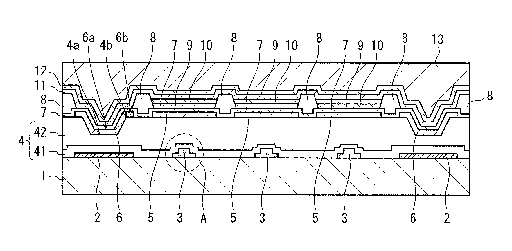
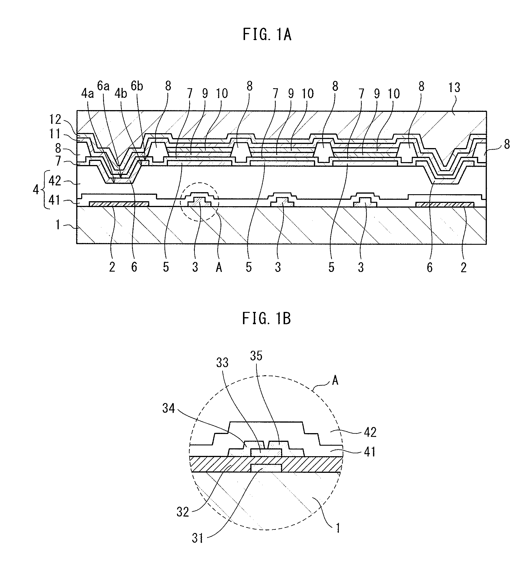
[0048]FIG. 1A is a cross-sectional diagram illustrating the configuration of an organic EL display panel pertaining to Embodiment 1 of the present disclosure, and FIG. 1B is a partial magnified view. Three pixels are shown.

[0049]The organic EL display panel includes a substrate 1, power supply wiring 2, thin-film transistors (hereinafter, TFTs) 3, an inter-layer insulation film 4, pixel electrodes 5, auxiliary wiring 6, a hole injection layer 7, a partition layer 8, a hole transport layer 9, an organic light-emitting layer 10, an electron transport layer 11, a common electrode 12, and a sealing layer 13.

[0050]The substrate 1 is made of an insulating material, such as glass or resin.

[0051]The power supply wiring 2 is arranged over the substrate 1. The material for the power supply wiring 2 may be any known wiring material having conductivity.

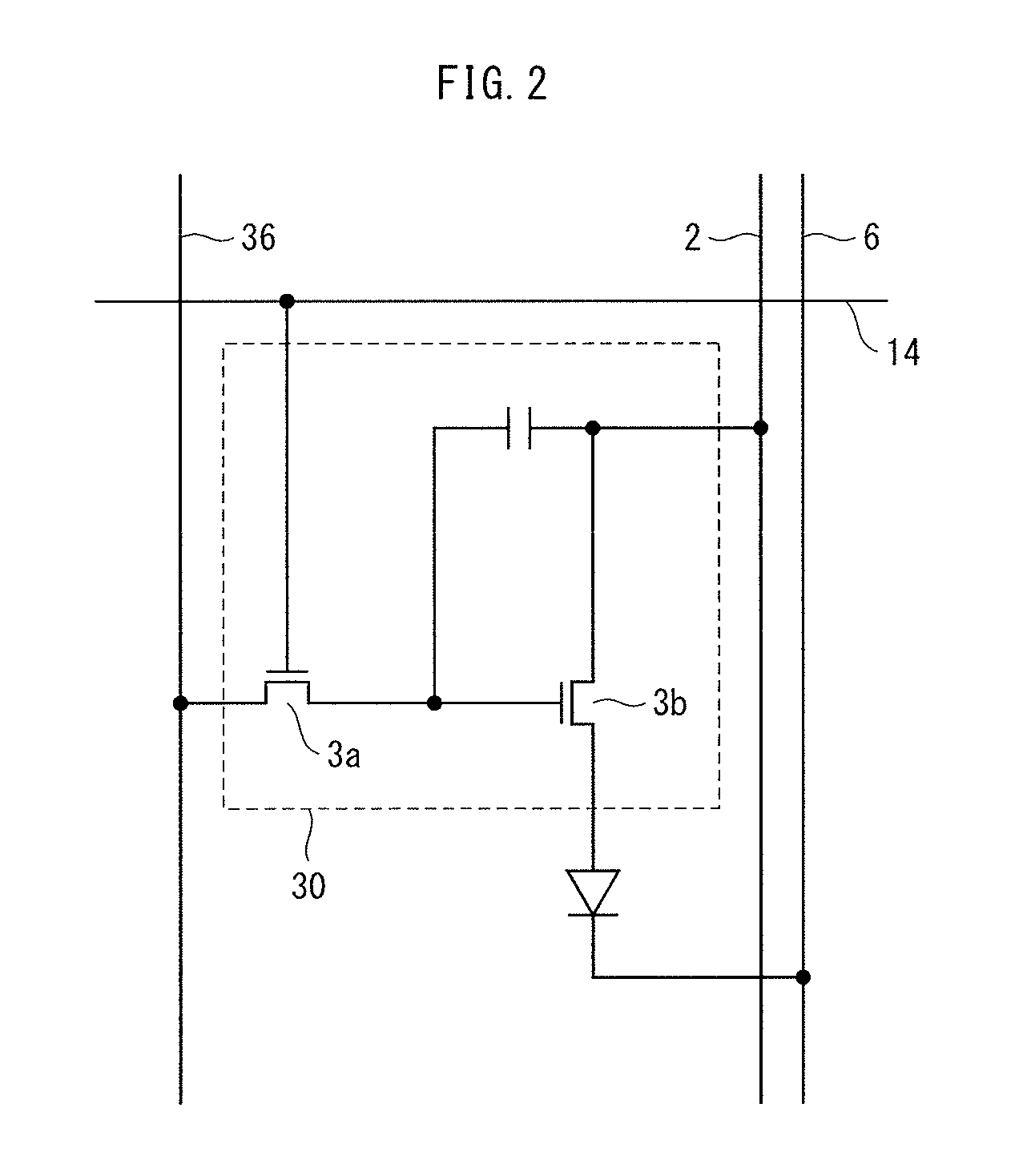
[0052]The TFTs 3 are arranged over the substrate 1. As shown in the magnified view of portion A, each of the TFTs 3 include...

embodiment 2

[0083]Embodiment 2 differs from Embodiment 1 in the shape used for the concave portions 6a of the auxiliary wiring 6. Otherwise, Embodiment 2 is identical to Embodiment 1, and explanations are therefore omitted.

[0084]FIG. 9 shows a plan view of the organic EL display panel pertaining to Embodiment 2, including pixel electrodes, auxiliary wiring, the partition layer, and scan lines. In the present Embodiment, the concave portions 6a of the auxiliary wiring 6 each include a first groove 6al aligned with the auxiliary wiring 6 and second grooves 6a2 each intersecting one of the first grooves 6a1. The second grooves 6a2 each have width W2, which is longer than width W1 of the first grooves 6a1. Similarly, the second grooves 6a2 each have length W3, which is longer than width W1 of the first grooves 6a1. FIG. 10A is a cross-section taken along line A1-A1 of FIG. 9, and FIG. 10B is a cross-section taken along line A2-A2 of FIG. 9. The first grooves 6a1 and the second grooves 6a2 have the ...


PUM


Abstract

A organic EL display panel includes an inter-layer insulation film, a pixel electrode, auxiliary wiring, a partition layer, an organic light-emitting layer, and a common electrode. The inter-layer insulation film has at least one paired concave portion and non-concave portion disposed in a region over the auxiliary wiring, a top face of the concave portion being concave with respect to a top face of the non-concave portion, and the auxiliary wiring includes a part over the concave portion and a part over the non-concave portion, a top face of the part over the concave portion being concave with respect to a top face of the part over the non-concave portion.

Description

TECHNICAL FIELD[0001]The present invention pertains to an organic electroluminescence display panel (hereinafter, organic EL display panel) and to a manufacturing method for same, and particularly pertains to auxiliary wiring for diminishing a voltage drop toward the centre of the panel.BACKGROUND ART[0002]Presently, research and development are advancing in organic EL display panel of the active matrix type, where each pixel is provided with an organic electroluminescence element (hereinafter, organic EL element) along with a drive circuit to drive the organic EL element. The organic EL element includes a bottom electrode, a top electrode, and an organic light-emitting layer disposed between the electrodes, as well as a functional layer that includes a hole injection layer, a hole transport layer, an electron injection layer, an electron transport layer, and so on as needed. Typically, an organic EL display panel has a common electrode as the top electrode provided in common for al...

Claims


Application Information

Patent Timeline
Patent Type & Authority Applications(United States)
IPC IPC(8): H01L27/32H01L51/56
CPCH01L27/3279H01L2227/323H01L27/3258H01L51/56H10K59/1315H10K59/122H10K50/824H10K59/1201H10K59/124H10K71/00
Inventor NENDAI, KENICHIOSAKO, TAKASHIMIZUSAKI, NAOKO
Owner JOLED INC
Why Eureka
Try Eureka