Semiconductor device and inverter device using the same

Active Publication Date: 2007-08-23
RENESAS ELECTRONICS CORP
View PDF10 Cites 29 Cited by
  • Summary
  • Abstract
  • Description
  • Claims
  • Application Information

AI Technical Summary

Benefits of technology

[0024] According to the present invention, since an avalanche current is prevented from flowing due to breakdown of the IGBT when a reverse voltage is applied to a low-cost and low-loss

Problems solved by technology

Therefore, there is a problem that the junction of the p-type emitter layer and the

Method used


Image

  • Semiconductor device and inverter device using the same
  • Semiconductor device and inverter device using the same
  • Semiconductor device and inverter device using the same

Examples


Example

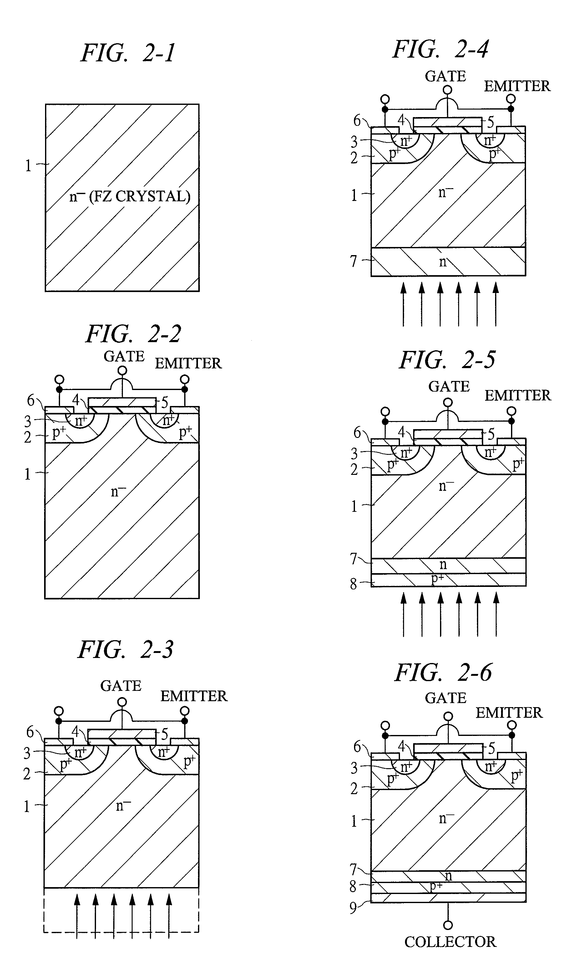
[0047] Hereinafter, embodiments of the present invention will be described in detail with reference to the accompanying drawings. Note that components having the same function are denoted by the same reference symbols throughout the drawings for describing the embodiment, and the repetitive description thereof will be omitted.

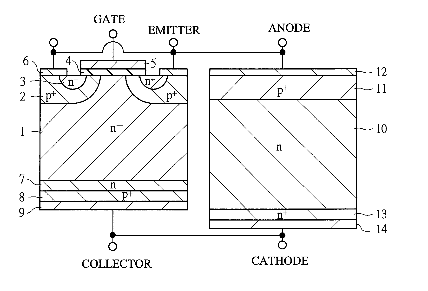
[0048]FIG. 1 shows a sectional structure and a connection relationship of an IGBT and a diode in a semiconductor device (IGBT module) of an embodiment applied with the present invention.

[0049] The semiconductor device of the embodiment includes one pair of an IGBT and a diode.

[0050] The IGBT is composed of a first FZ crystal, and has a pair of principal surfaces and an exposed surface on a first principal surface on a collector-electrode side. Incidentally, a second principal surface is positioned on an insulated gate-electrode side.

[0051] This IGBT is formed in an area including: a p-type emitter layer (first region) 8; an n-type buffer layer (second regio...


PUM


Abstract

In a semiconductor device having a pair of IGBT and diode which are connected to each other in inverse-parallel in which a collector-electrode of the IGBT and a cathode-electrode of the diode are wired to each other, and an emitter-electrode of the IGBT and an anode-electrode of the diode are wired to each other, when a breakdown voltage of a junction of a p-type emitter layer and an n-type buffer layer of the IGBT is represented as BVec, and a forward voltage occurring while the diode transits from a state of blocking to a state of forward conduction is represented as VF, a relationship of VF<BVec is satisfied in a predetermined current value Id of a current flowing in the diode, and the maximal doping concentration of the n-type cathode layer of the diode is higher than that of the n-type buffer layer of the IGBT.

Description

CROSS-REFERENCE TO RELATED APPLICATION [0001] The present application claims priority from Japanese Patent Application No. JP 2006-043255 filed on Feb. 21, 2006, the content of which is hereby incorporated by reference into this application. TECHNICAL FIELD OF THE INVENTION [0002] The present invention relates to a technique for a semiconductor device. More particularly, to a technique effectively applied to a semiconductor device in which an insulated gate bipolar transistor and a diode are connected to each other in inverse-parallel (hereinafter, it is abbreviated as an IGBT module). BACKGROUND OF THE INVENTION [0003] An insulated gate bipolar transistor (IGBT) is a switching element controlling a current applied between a collector-electrode and an emitter-electrode by a voltage applied to a gate-electrode. A controllable power of the switching element extends from tens of watts to hundreds of thousands of watts, and a switching frequency thereof also has such a wide range from t...

Claims


Application Information

Patent Timeline
IPC IPC(8): H01L29/74
CPCH01L21/268H01L29/861H01L29/7395H01L27/0664
Inventor NAGASE, TAKUOMORI, MUTSUHIRO
Owner RENESAS ELECTRONICS CORP
Why Eureka
Try Eureka