Grain growth promotion layer for semiconductor interconnect structures

Active Publication Date: 2007-08-23
IBM CORP
View PDF27 Cites 56 Cited by
  • Summary
  • Abstract
  • Description
  • Claims
  • Application Information

AI Technical Summary

Benefits of technology

[0006] The present invention provides an interconnect structure of the single or dual damascene type and a method of forming the same, which substantially reduces the electromigration problem that is exhibited by prior art interconnect structures. In accordance with

Problems solved by technology

One major problem with prior art interconnect structures is that the conductive material within the conductive region has a low electromigration resistance due to a high number o

Method used


Image

  • Grain growth promotion layer for semiconductor interconnect structures
  • Grain growth promotion layer for semiconductor interconnect structures
  • Grain growth promotion layer for semiconductor interconnect structures

Examples


Embodiment Construction

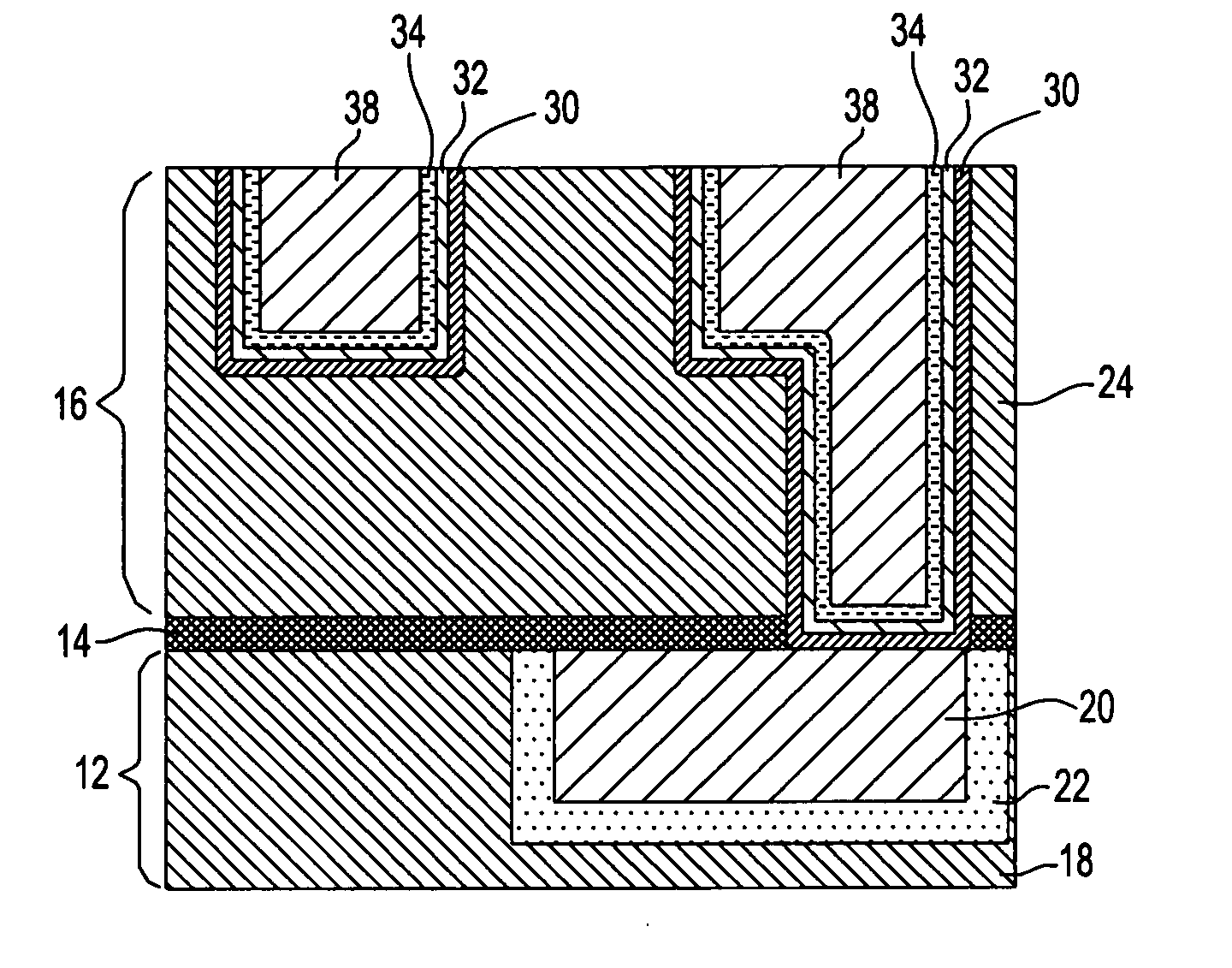
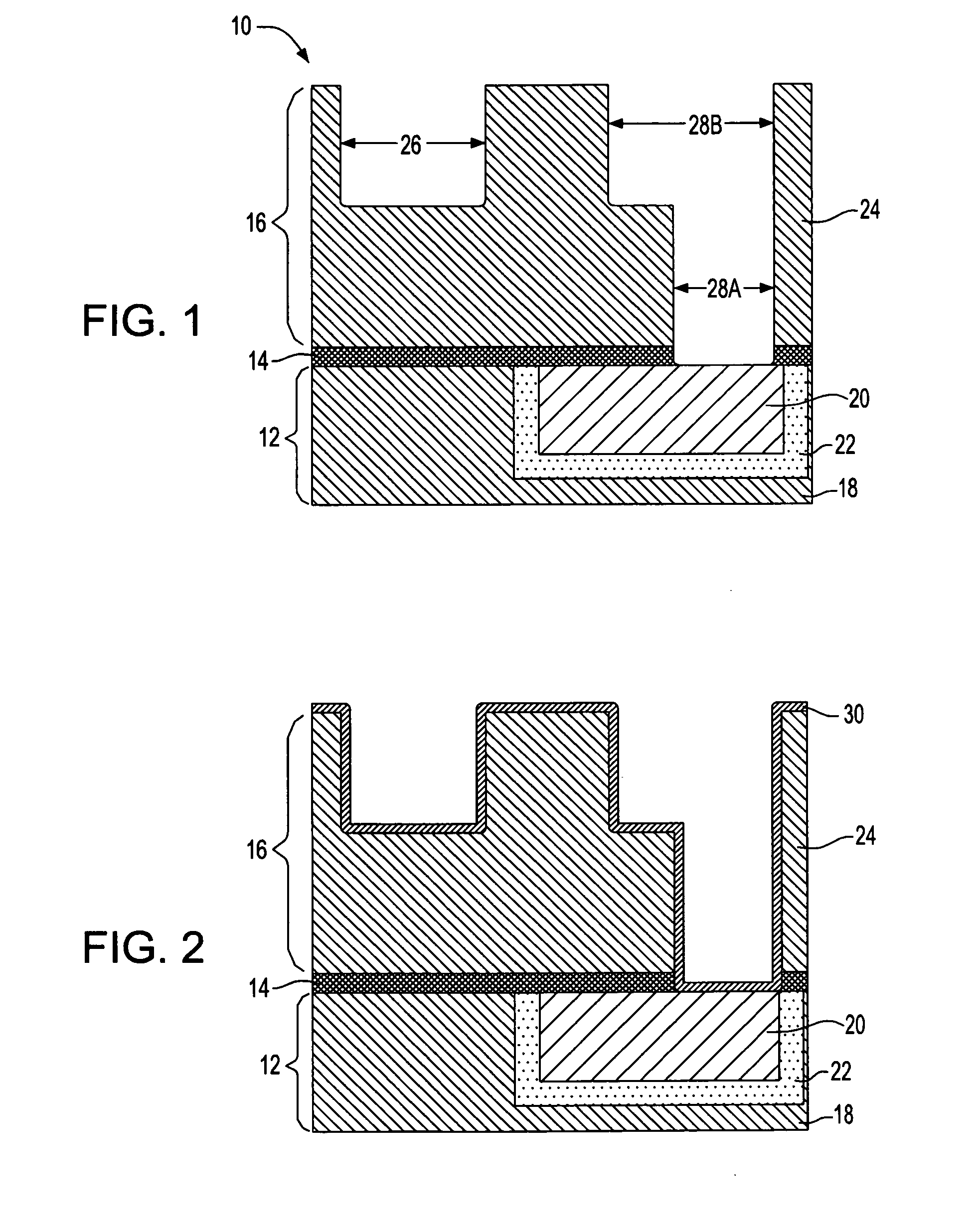
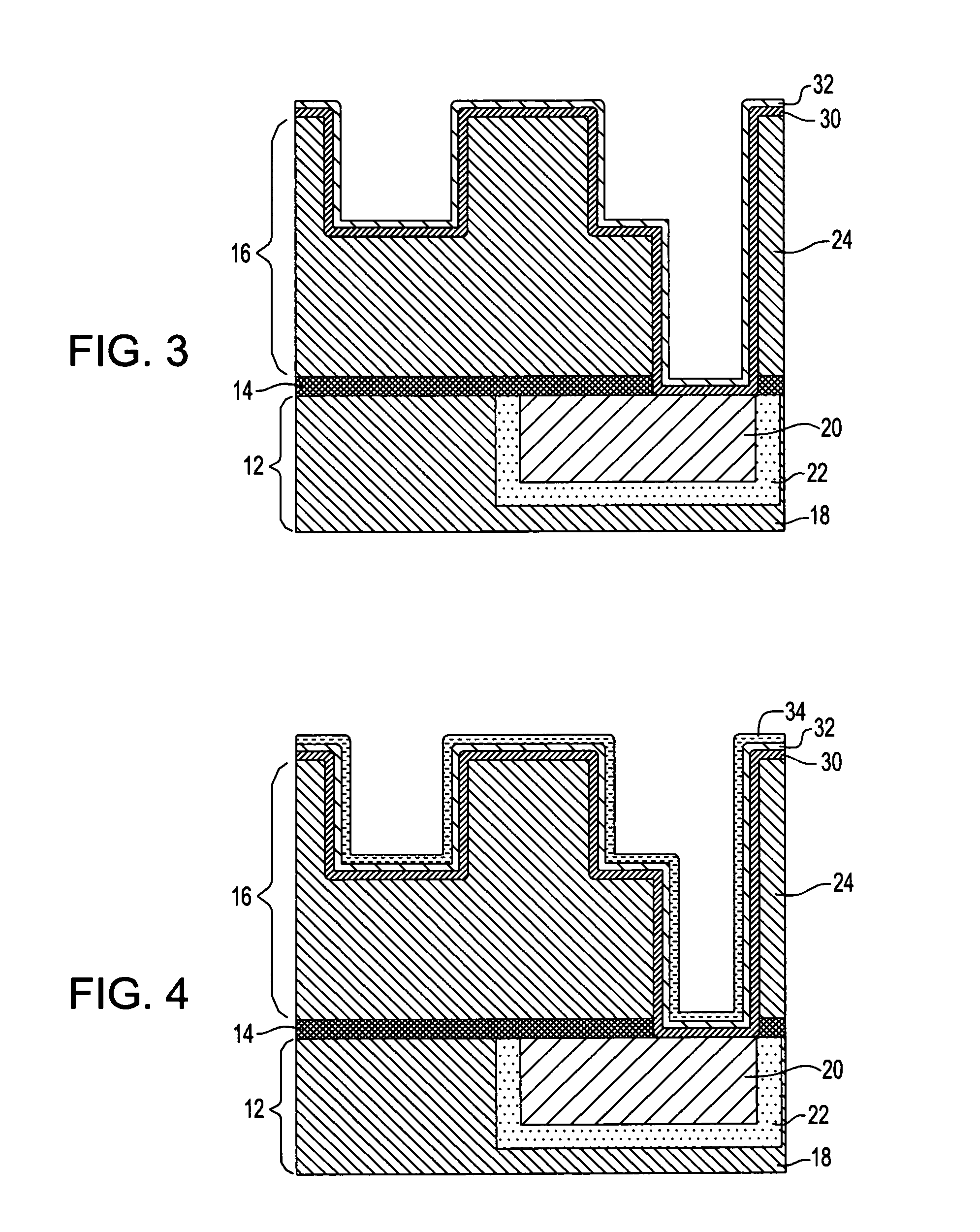
[0022] The present invention, which provides an interconnect structure including a grain growth promotion layer and a conductive region having a bamboo microstructure and an average grain size larger than 0.05 microns and a method of fabricating the same, will now be described in greater detail by referring to the following discussion and drawings that accompany the present application. The drawings of the present application, which are referred to herein below in greater detail, are provided for illustrative purposes and, as such, they are not drawn to scale.

[0023] The process flow of the present invention begins with providing the initial interconnect structure 10 shown in FIG. 1. Specifically, the initial interconnect structure 10 shown in FIG. 1 comprises a multilevel interconnect including a lower interconnect level 12 and an upper interconnect level 16 that are separated in part by dielectric capping layer 14. The lower interconnect level 12, which may be located above a semi...


PUM


Abstract

An interconnect structure of the single or dual damascene type and a method of forming the same, which substantially reduces the electromigration problem that is exhibited by prior art interconnect structures, are provided. In accordance with the present invention, a grain growth promotion layer, which promotes the formation of a conductive region within the interconnect structure that has a bamboo microstructure and an average grain size of larger than 0.05 microns is utilized. The inventive structure has improved performance and reliability.

Description

FIELD OF THE INVENTION [0001] The present invention relates to a semiconductor structure and a method of fabricating the same. More particularly, the present invention relates to an interconnect structure of the single or dual damascene type in which a grain growth promotion layer is used to provide a conductive region within the interconnect structure that has a bamboo microstructure and an average grain size of larger than 0.05 microns. The presence of the conductive region having such a microstructure and a relatively large average grain size results in a structure that has enhanced performance and reliability. The present invention also relates to a method of fabricating such a semiconductor structure. BACKGROUND OF THE INVENTION [0002] Generally, semiconductor devices include a plurality of circuits which form an integrated circuit fabricated on a semiconductor substrate. A complex network of signal paths will normally be routed to connect the circuit elements distributed on th...

Claims


Application Information

Patent Timeline
IPC IPC(8): H01L21/44
CPCH01L21/76805H01L21/76843H01L21/76844H01L21/76877H01L23/5226H01L23/53238H01L2924/0002H01L23/5329H01L23/53295H01L2924/00
Inventor YANG, CHIH-CHAOPONOTH, SHOM
Owner IBM CORP
Why Eureka
Try Eureka