OLED device having improved light output

Active Publication Date: 2007-08-30
GLOBAL OLED TECH
View PDF12 Cites 80 Cited by
  • Summary
  • Abstract
  • Description
  • Claims
  • Application Information

AI Technical Summary

Benefits of technology

[0020] The present invention has the advantage that it increases th

Problems solved by technology

However, as is well known, much of the light output from the light-emissive layer in the OLED is absorbed within the device.
In general, up to 80% of the light may be lost in this manner.
It has been found, however, that one of the key factors that limits the efficiency of OLED devices is the inefficiency in extracting the photons generated by the electron-hole recombination out of the OLED devices.
Due to the high optical indices of the organic materials used, most of the photons generated by the recombination process are actually trapped in the devices due to total internal reflection.
However, scattering techniques, by themselves, cause light to pass through the light-absorbing material layers multiple times where they are absorbed and converted to heat.
Moreover, trapped light may propagate a considerable distance hori

Method used


Image

  • OLED device having improved light output
  • OLED device having improved light output
  • OLED device having improved light output

Examples


Embodiment Construction

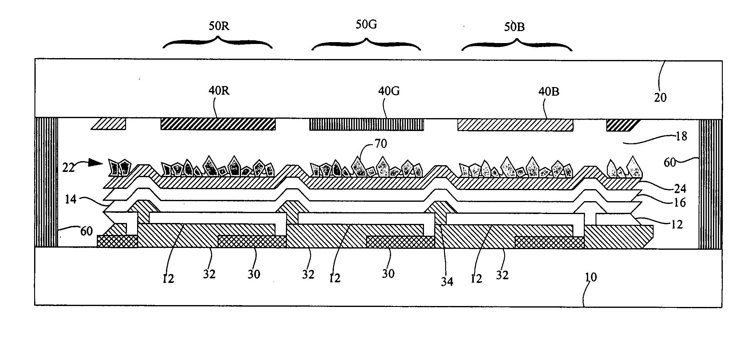
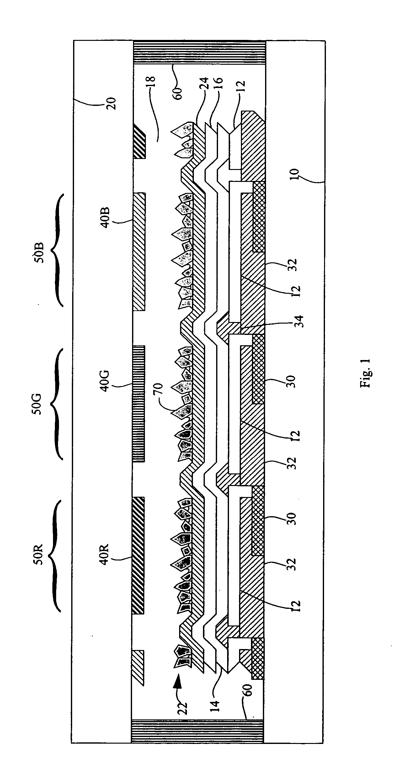
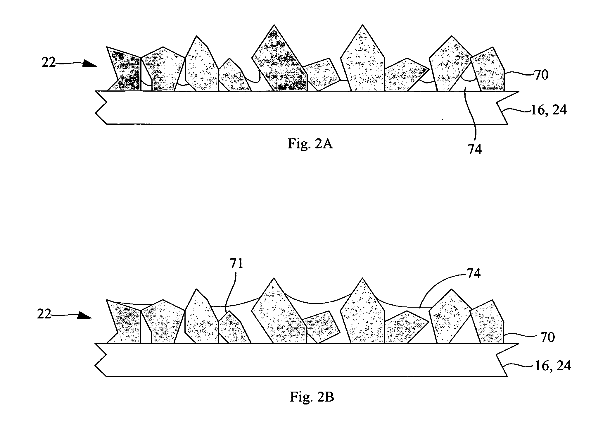
[0028] Referring to FIG. 1, in accordance with one embodiment of the present invention, a top-emitting organic light-emitting diode (OLED) device, comprises a substrate 10; an OLED comprising a reflective electrode 12 formed on the substrate 10; one-or-more layers 14 of organic light-emitting material formed over the reflective electrode 12; and a transparent electrode 16 formed over the one-or-more layers 14 of organic light-emitting material; a light-scattering layer 22 having a rough surface formed over and in contact with the OLED; a cover 20 affixed to the substrate 10 forming a gap 18 between the cover 20 and the light scattering layer 22; and wherein the gap 18 is a vacuum or the gap 18 is filled with a relatively low-refractive index gas and the light-scattering layer 22 comprises a plurality of relatively high-refractive index light-scattering transparent particles 70 projecting into the gap 18 without contacting the cover 20 and further comprising an adhesive binder in con...


PUM


Abstract

A top-emitting organic light-emitting diode (OLED) device, comprising: a substrate; an OLED comprising a reflective electrode formed on the substrate; one-or-more layers of organic light-emitting material formed over the reflective electrode; and a transparent electrode formed over the one-or-more layers of organic light-emitting material; a light-scattering layer having a rough surface formed over and in contact with the OLED, a cover affixed to the substrate forming a gap between the cover and the light scattering layer; and wherein the gap is a vacuum or the gap is filled with a relatively low-refractive index gas and the light-scattering layer comprises a plurality of relatively high-refractive index light-scattering transparent particles projecting into the gap without contacting the cover and further comprising an adhesive binder in contact with at least some of the light-scattering particles to adhere the light-scattering particles to the OLED.

Description

FIELD OF THE INVENTION [0001] The present invention relates to organic light-emitting diode (OLED) devices, and more particularly, to OLED device structures for improving light output and reducing manufacturing costs. BACKGROUND OF THE INVENTION [0002] Organic light-emitting diodes (OLEDs) are a promising technology for flat-panel displays and area illumination lamps. The technology relies upon thin-film layers of materials coated upon a substrate. However, as is well known, much of the light output from the light-emissive layer in the OLED is absorbed within the device. Because light is emitted in all directions from the internal layers of the OLED, some of the light is emitted directly from the device, and some is emitted into the device and is either reflected back out or is absorbed, and some of the light is emitted laterally and trapped and absorbed by the various layers comprising the device. In general, up to 80% of the light may be lost in this manner. [0003] OLED devices ge...

Claims


Application Information

Patent Timeline
IPC IPC(8): H05B33/04H01J1/62
CPCH01L51/5237H01L2251/5315H01L51/5268H10K50/841H10K50/854H10K50/844H10K2102/3026
Inventor COK, RONALD S.WANG, JIN-SHANKESEL, RAYMOND A.PREUSS, DONALD R.TYAN, YUAN-SHENG
Owner GLOBAL OLED TECH
Why Eureka
Try Eureka