Contact pusher, contact arm, and electronic device test apparatus

a test apparatus and pusher technology, applied in the direction of measurement devices, semiconductor/solid-state device testing/measurement, instruments, etc., can solve the problems of unstable heat conductivity of ic devices, liable to be warped along with excessive pushing, and ic devices b>10/b> is liable not to be suitably given the desired thermal stress, etc., to achieve stable heat conductivity

Inactive Publication Date: 2007-08-30
ADVANTEST CORP
View PDF6 Cites 27 Cited by
  • Summary
  • Abstract
  • Description
  • Claims
  • Application Information

AI Technical Summary

Benefits of technology

[0010]An object of the present invention is to provide a contact pusher able to stably conduct heat and suitably apply thermal stress without being affected by variations in the shape of the electronic device under test and to provide a contact arm and electronic device test apparatus provided with the same.
[0012]In the present invention, the first pushing means can be brought into contact with the heat conducting means and moved finely along the pushing direction. By finely moving the first pushing means, it becomes possible to absorb variations in dimensions of the electronic device under test in the height direction. Further, by bringing the first pushing means into contact with the heat conducting means, it is possible to suitably apply thermal stress to the electronic device under test.

Problems solved by technology

However, when there are variations in the thickness of the package 11 or height of the terminals 12 in the IC device 10 under test, the IC device 10 is liable not to be suitably given the desired thermal stress or the terminals 12 are liable to be warped along with excessive pushing.
Therefore, the heat conducted to the IC device 10a will become unstable.
As a result, there is the problem that the temperature will be insufficiently applied and a stable test quality will no longer be obtained in the device test.
Further, there is the problem that the terminals 12 will be excessively pushed resulting in the terminals 12 being bent.
Therefore, there is the problem that the terminals 12 will be bent by being excessively pressed by the contact pins 320 of the contact part 310.

Method used


Image

  • Contact pusher, contact arm, and electronic  device test apparatus
  • Contact pusher, contact arm, and electronic  device test apparatus
  • Contact pusher, contact arm, and electronic  device test apparatus

Examples


first embodiment

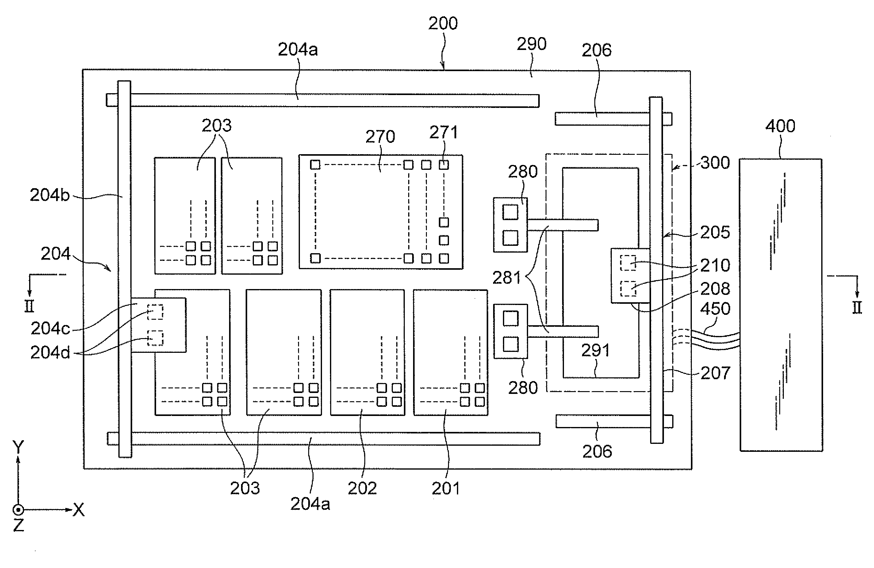
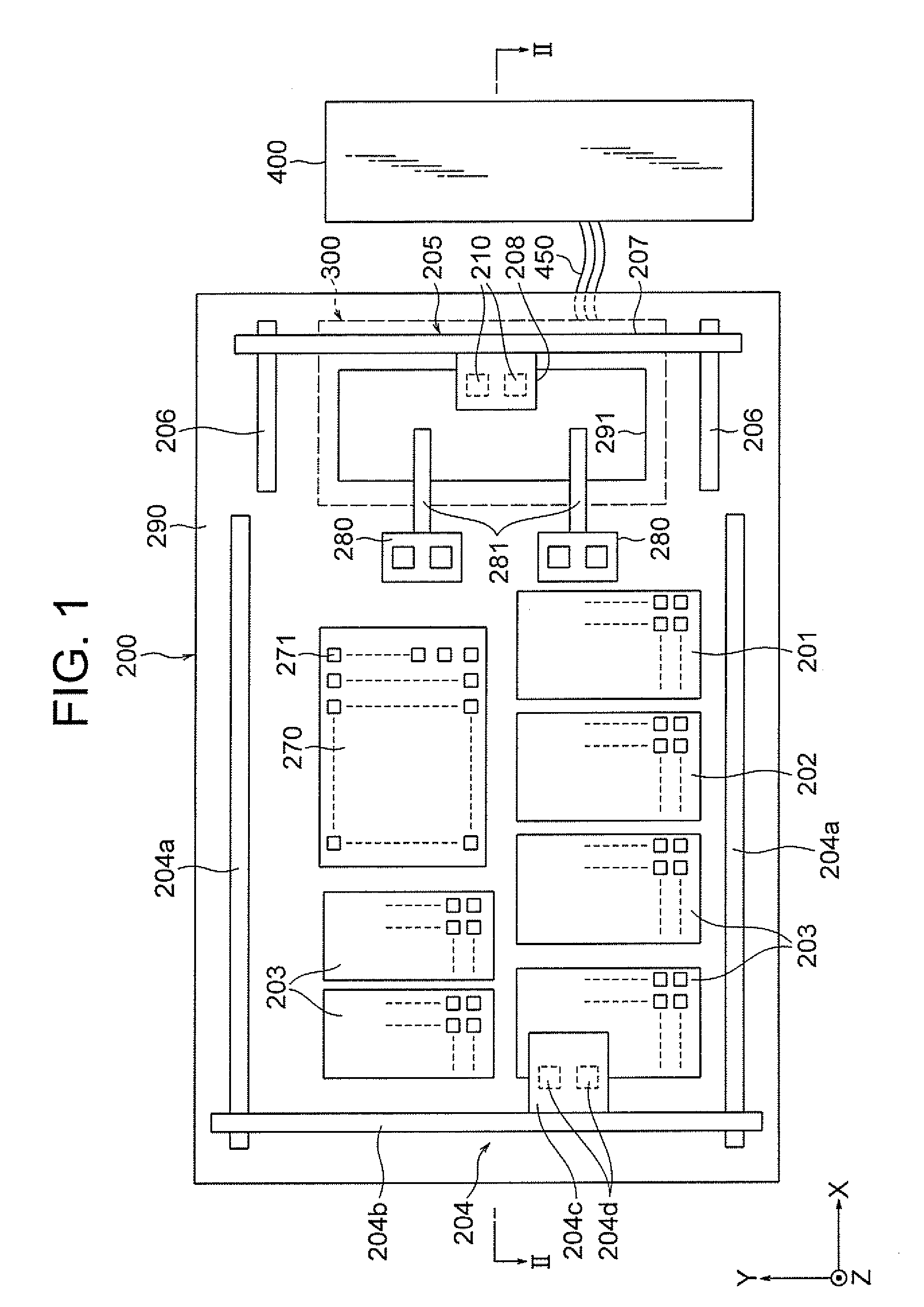
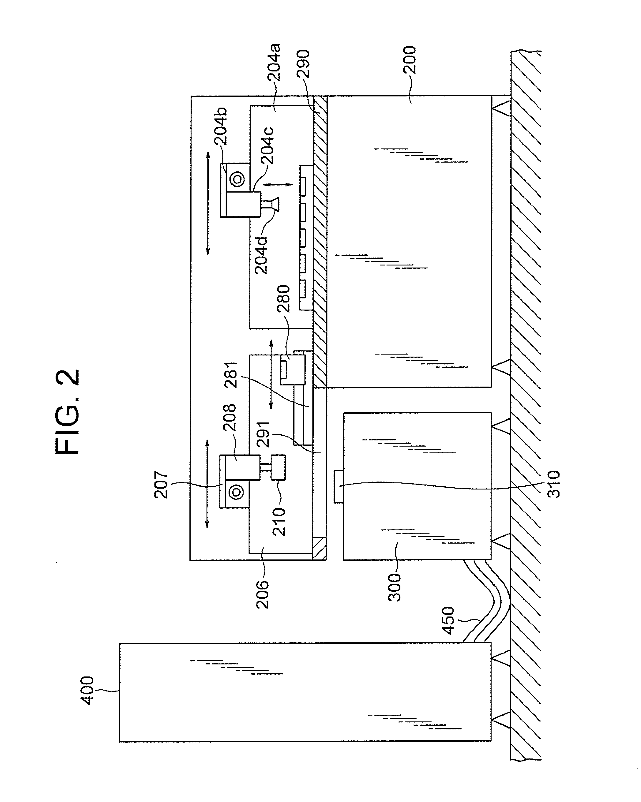
[0043]An electronic device test apparatus 200 according to a first embodiment of the present invention is a logic IC test apparatus for testing logic ICs. As shown in FIG. 1, it is provided with various types of trays 201 to 203, XY movement systems 204, 205, a heat plate 270, and buffer parts 280 and IC devices 10 are tested by using a test head 300 and a tester 400. The test head 300 and the tester 400 are connected through a cable 450.

[0044]This electronic device test apparatus 200 pushes IC devices 10 before test carried in on a feed tray 202 by the XY movement systems 204, 205 against contact parts 310 of the test head 300, has the tester 400 test the IC devices 10 through this test head 300 and cable 450, then stores the IC devices 10 finished being tested on classification trays 203 in accordance with the test results.

[0045]The apparatus board 290 of this electronic device test apparatus 200 is provided on it with XY movement systems 204, 205. Further, the apparatus board 290...

second embodiment

[0074]The contact pusher 220d according to a second embodiment of the present invention, as shown in FIG. 8, differs from the contact pusher 220a according to the first embodiment only on the point that no second springs 237 are interposed between the base part 230 and the first press part 250. The rest of the configuration is similar to that of the contact pusher 220a according to the first embodiment.

[0075]As shown in the present embodiment, it is also possible not to provide the second springs 237, but to use the weight of the first press part 250 to make first press part 250 closely contact the top surface of the package 11 of the IC device 10 during pushing. Due to this, it is possible to make the base part 230 and the first press part 250 heat conductible in state and possible to finely move the first press part 250 along the vertical direction.

third embodiment

[0076]The contact pusher 220c according to a third embodiment of the present invention, as shown in FIG. 9, differs from the contact pusher 220a according to the first embodiment only on the point that instead of the first springs 257 interposed between the first press part 250 and second press part 26, suction pads 238 branching off from the tube 241 and drawing the pushers 251 toward them are provided. The rest of the configuration is similar to that of the contact pusher 220a according to the first embodiment.

[0077]In the present embodiment, as shown in FIG. 9, the base part 230 is formed with channels 239 passing through from the through hole 231 to the outer circumferential surface 232a of the bottom projecting part 232. The front end of each channel 239 at the outer circumferential surface 232a side is provided with a suction pad 238 opening toward the outside.

[0078]Each channel 239 formed in the base part 230 is communicated with a channel 242 of the tube 241 inserted in the ...


PUM


Abstract

A contact pusher (220a) attached to the front end of a contact arm (210) bringing an IC device (10) into contact with a contact part of a test head and pushing the IC device (10) is provided with a suction pad (240) for picking up and holding an IC device (10), a first press part (250) for pushing against a package (11) of an IC device (10), a second press part (260) for pushing against terminals (12) of the IC device (10), and a base part (230) for conducting heat to the first press part (250), the first press part (250) and the base part (230) contacting each other and the first press part (250) provided to be able to finely move relative to the base part (230).

Description

TECHNICAL FIELD[0001]The present invention relates to a contact pusher attached to the front end of a contact arm bringing a semiconductor integrated circuit or other type of electronic device (below, also referred to representatively as an “IC device”) into contact with a contact part of a test head and pushing against the IC device and to a contact arm and electronic device test apparatus provided with the same.BACKGROUND ART[0002]In the process of production of an IC device or other electronic device, an electronic device test apparatus is used to test the performance and functions of the IC device in the packaged state.[0003]In a handler forming part of the electronic device test apparatus, a large number of IC devices carried a tray are placed in the handler. While applying high temperature thermal stress, the input / output terminals of each IC device are brought into electrical contact with the contact part of the test head for testing at the electronic device test apparatus ma...

Claims


Application Information

Patent Timeline
Patent Type & Authority Applications(United States)
IPC IPC(8): G01R31/28G01R31/26H01L21/66
CPCG01R31/2893G01R31/2887G01R31/26H01L22/00
Inventor MIZUSHIMA, AYUMUOGURA, JUN
Owner ADVANTEST CORP
Why Eureka
Try Eureka