Magnetoresistive random-access memory device

a random access and memory device technology, applied in the direction of instruments, spin-exchange-coupled multilayers, substrate/intermediate layers, etc., can solve the problems of increased cost and chip size, gmr memory is used, and difficult reading operation, so as to improve the heat resistance of the tmr element, improve the mr ratio, and high-integrated mram

Inactive Publication Date: 2006-08-10
JAPAN SCI & TECH CORP
View PDF4 Cites 17 Cited by
  • Summary
  • Abstract
  • Description
  • Claims
  • Application Information

AI Technical Summary

Benefits of technology

[0046] While the conventional MRAM is essentially required to have the MOS transistor with the switching function for selecting an intended memory element, the present invention can provide a MRAM in a simplified structure without any MOS transistor by use of a p-n junction spin-rectifier diode or p-i-n junction spin-rectifier diode formed of half-metallic ferromagnetic semiconductors. Thus, the present invention makes it possible to develop a highly integrated MRAM. In addition, the MRAM of the present invention has no need for the aforementioned production process for the MOS transistor, and thereby can be processed at a high temperature.
[0047] At present, a TMR element using a thin film of metallic ferromagnetic material has a MR rate of about 50%, and this MR rate is not varied depending on the dimensions of the TMR element. Instead of the thin film of metallic ferromagnetic material, the present invention employs the p-type and n-type half-metallic ferromagnetic semiconductor thin films to open the way for developing a high-performance MRAM having a significantly increased MR ratio.
[0048] As to a heat stability of the TMR element using a thin film of metallic ferromagnetic material, while a maximum MR rate is achieved at an annealing temperature of 300° C., the conventional MRAM has to be typically subjected to a heat treatment at a temperature of 400° C. in a hydrogen atmosphere to recover damages in a CMOS transistor due to microfabrication and / or patterning of metal wirings. During this heat treatment, the MR rate of the TMR element becomes zero. Thus, it is required to improve the heat resistance of the TMR element or reduce the temperature for the heat treatment of the CMOS transistor. The MRAM of the present invention including no MOS transistor can be processed at a high temperature during production process. That is, the heat stability of the half-metallic ferromagnetic semiconductor-based TMR element is sufficient to positively utilize a maximum MR ratio (100% to 500%) achieved at a high heat treatment temperature of 500° C. or more. Thus, as compared with the conventional MRAM based on the TMR element using a metal magnetic material, the half-metallic ferromagnetic semiconductor-based MRAM of the present invention can achieve extremely high performance and integration.

Problems solved by technology

Thus, an excessive increase in the number N causes difficulties in the reading operation due to disappearance of the signal voltage into noises.
Moreover, in the GMR element having a low resistance, a signal voltage itself is inherently low, and thereby it is required to provide a reading amplifier having a larger amplification capacity, which leads to increase in cost and chip size.
This is a problem in applications to customer devices, and consequently the GMR memory is used only as military and space devices under extremely limited conditions.
This is a realistic major issue in connection with achievement of a larger-capacity MRAM, and one of factors obstructive to practical use of the MRAM.
Thus, the memory cell size per bit is increased, and thereby it is difficult to achieve high-integration.
In contrast, one of reasons for difficulties in achieving a larger-capacity FeRAM is in that a ferroelectric film can be formed only at a high temperature of 500° C. or more.
This is a problem in developing a larger-capacity MRAM, and one of factors obstructive to practical use of the MRAM.
There is another problem about microfabrication for use in a thin film of metallic magnetic material.
Specifically, while the thin film is microfabricated through physical cutting by means of lithography and ion milling ion as a technique for research, such a technique cannot be applied to large-scale productions.

Method used


Image

  • Magnetoresistive random-access memory device
  • Magnetoresistive random-access memory device
  • Magnetoresistive random-access memory device

Examples


example

Example 1

[0076]—Preparation of MRAM Using n-type (Ga, Cr) N and p-type (Ga, Mn) N Half-Metallic Dilute Ferromagnetic Semiconductors—

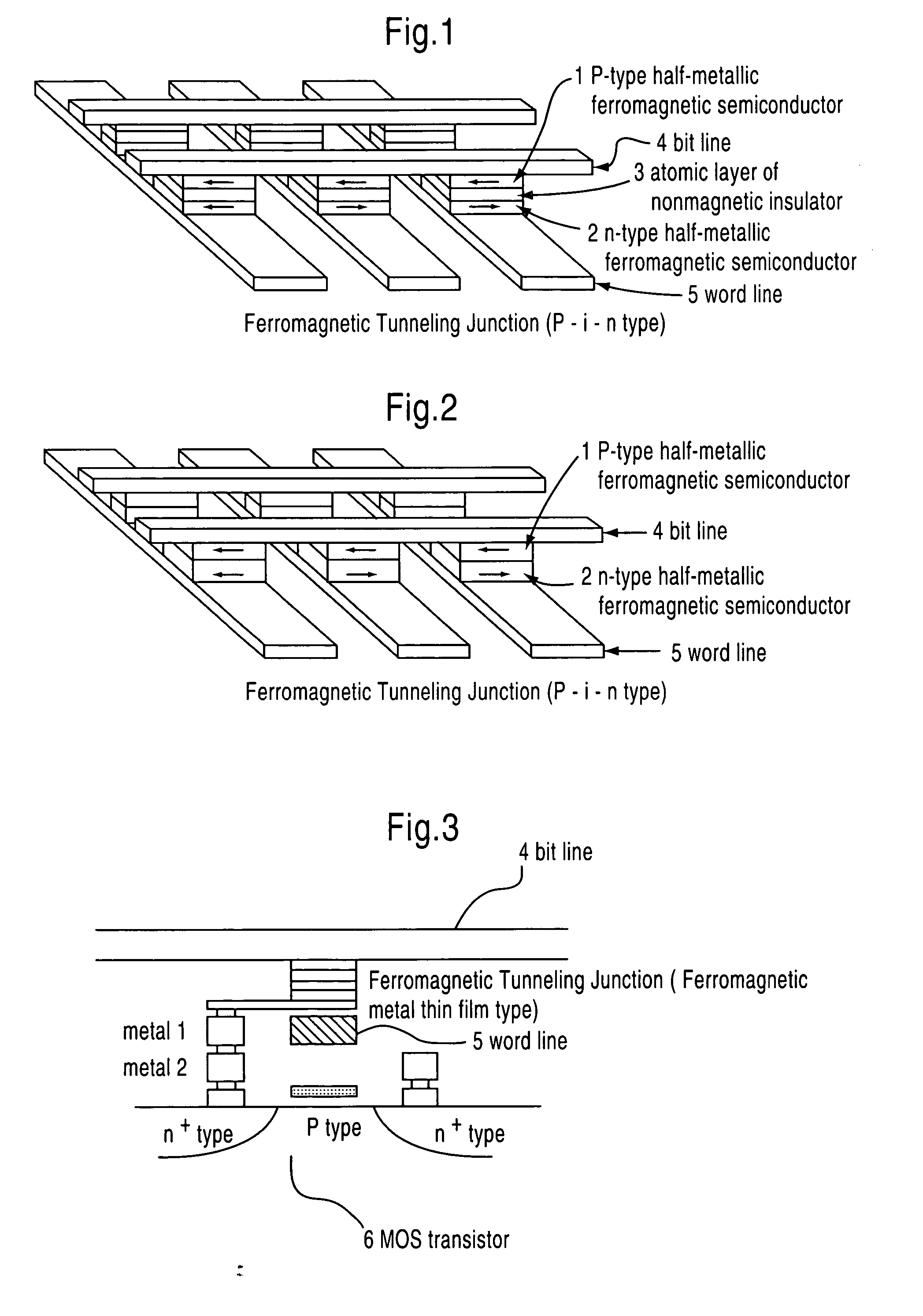
[0077] In order to reduce the resistance of a TMR element, a p-i-n type low-resistance tunneling-magnetoresistance-effect (low-resistance TMR) diode was prepared using p-type (Ga, Mn) N (the concentration of Mn: 10 atomic %) as a p-type half-metallic dilute ferromagnetic semiconductor, n-type (Ga, Cr) N (the concentration of Cr: 10 atomic %) as an n-type half-metallic dilute ferromagnetic semiconductor, and two atomic layers of nonmagnetic insulator GaN (i-layers) interposed therebetween, as shown in FIG. 1.

[0078] It was verified that the new type of TMR element exhibits a rectification effect of allowing a rectified current to flow in only one direction in response to applying a low voltage of 5 to 20 meV to bit and word lines. This means that a new type of magnetoresistive random-access memory (MRAM) using p-type and n-type half-metallic dilute ferr...

example 2

[0082]—Preparation of MRAM Using n-Type (Zn, V) O and p-Type (Zn, Cr) O Half-Metallic Dilute Ferromagnetic Semiconductors—

[0083] In order to reduce the resistance of a TMR element, a p-i-n type low-resistance tunneling-magnetoresistance-effect (low-resistance TMR) diode was prepared using p-type (Zn, Cr) N (the concentration of Cr: 10 atomic %) as a p-type half-metallic dilute ferromagnetic semiconductor, n-type (Zn, V) N (the concentration of V: 10 atomic %) as an n-type half-metallic dilute ferromagnetic semiconductor, and three atomic layers of nonmagnetic insulator ZnO (i-layers) interposed therebetween, as shown in FIG. 1.

[0084] It was verified that the new type of TMR element exhibits a rectification effect of allowing a rectified current to flow in only one direction in response to applying a low voltage of 8 to 25 meV to bit and word lines. This means that a new type of magnetoresistive random-access memory (MRAM) using p-type and n-type half-metallic dilute ferromagnetic s...


PUM

PropertyMeasurementUnit
temperatureaaaaaaaaaa

Abstract

Disclosed is a new type of magnetoresistive random-access memory (MRAM) device using a magnetic semiconductor, which is capable of achieving high-integration and energy saving in a simplified structure without any MOS transistor, based on a rectification effect derived from a p-i-n type low-resistance tunneling-magnetoresistance-effect (low-resistance TMR) diode with a structure having a p-type half-metallic ferromagnetic semiconductor, an n-type half-metallic ferromagnetic semiconductor and at least one atomic layer of nonmagnetic insulator interposed therebetween, or a rectification effect derived from a p-n type low-resistance tunneling-magnetoresistance-effect (low-resistance TMR) diode with a structure devoid of the interposed atomic layer of nonmagnetic insulator.

Description

TECHNICAL FIELD [0001] The present invention relates to a new type of magnetoresistive random-access memory (MRAM) device which uses a p-n junction diode formed of half-metallic ferromagnetic semiconductor and includes no MOS transistor. BACKGROUND ART [0002] A conventional MRAM using a thin film of metallic magnetic material includes two types, one type utilizing a giant magnetoresistance effect (GMR) and the other type utilizing a tunneling magnetoresistance effect (TMR). An electrical resistance between two magnetic layers located adjacent to one another through a nonmagnetic layer is relatively low when the magnetization orientations of the two magnetic layers are parallel, and is increased when the magnetization orientations of the two magnetic layers are anti-parallel. These phenomenons are utilized to differentiate “1” and “0”, respectively. In a writing operation, a given current is supplied to each of a bit line and a word line to invert the magnetization orientation of the...

Claims


Application Information

Patent Timeline
Patent Type & Authority Applications(United States)
IPC IPC(8): H01L21/00H01L29/94H01L27/108H01L29/76H01L31/119G11C11/15H01F10/32H01L21/8246H01L27/105H01L43/08H01L43/12
CPCG11C11/15H10B61/00H10N50/85H10N50/10H01L27/105H10N50/01
Inventor YOSHIDA, HIROSHISATO, KAZUNORI
Owner JAPAN SCI & TECH CORP
Why Eureka
Try Eureka