

Delay management circuit for reading out large S/H arrays
a delay management and array technology, applied in the field of cmos image sensors, can solve the problems of reducing the effective read-out time, noise at the output of the column s/h array, and causing the decoder to delay with larger and larger delays, so as to reduce the mis-sampling of the s/h circuit and increase the effective sensor read-out speed
- Summary
- Abstract
- Description
- Claims
- Application Information
AI Technical Summary
Benefits of technology
Problems solved by technology
Method used
Image

Examples
Embodiment Construction
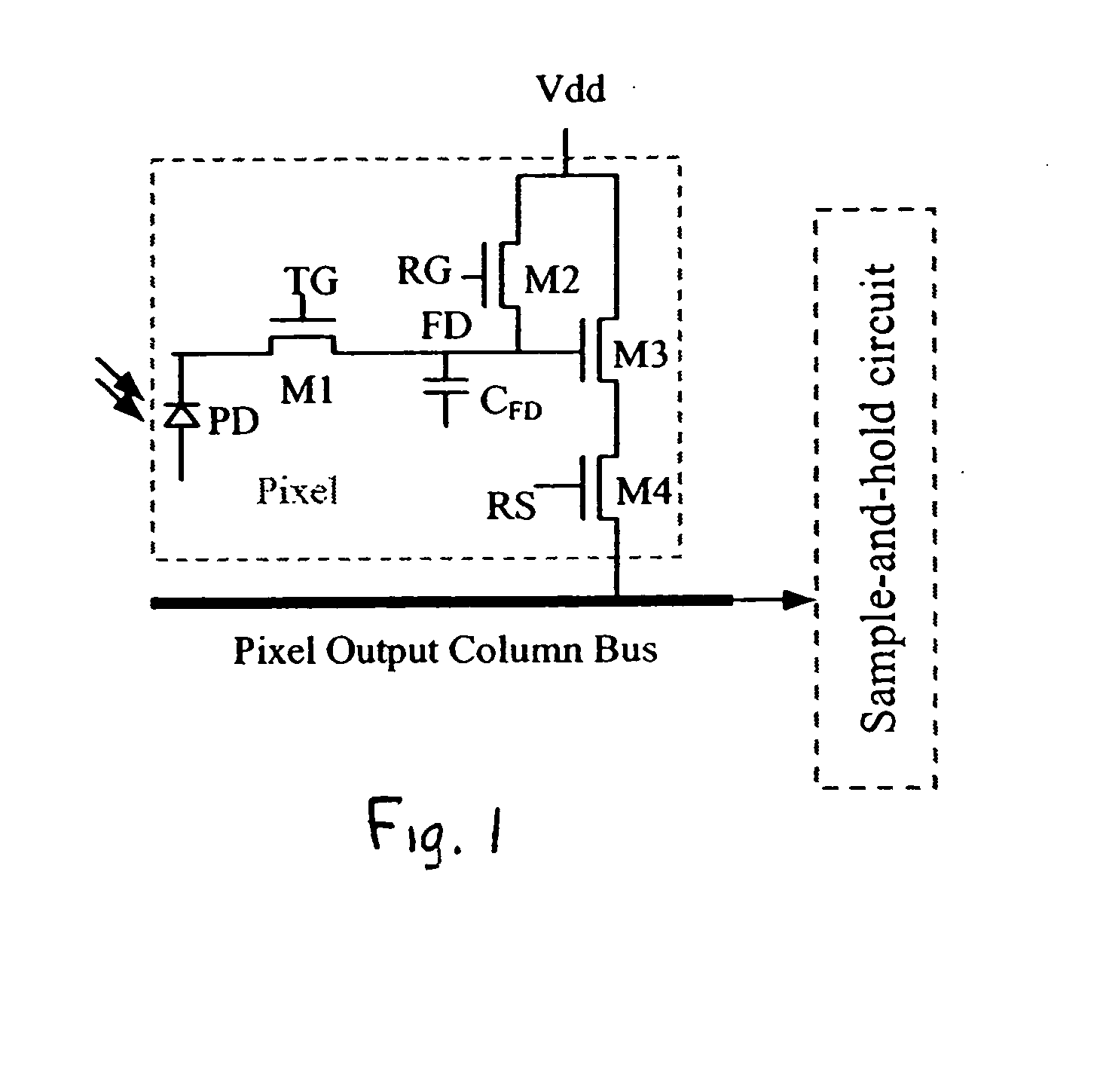
[0012]FIG. 1 shows a typical 4-transistor CMOS active image sensor pixel. A photodiode PD collects charge in response to incident light. Transistor M1 is controlled by a voltage applied on its gate TG to transfer the charge accumulated in PD to the floating diffusion capacitor CFD when TG is “high”. Floating diffusion capacitor CFD converts the charge to voltage. Transistor M2 resets the floating diffusion capacitor CFD when a “high” voltage is applied to its gate RG. The selectable pixel output buffer amplifier is composed of M3 and M4. M3 is the amplifier input transistor and M4 is the row-selecting transistor to enable the amplifier. The voltage at the floating diffusion FD is applied to the input of the pixel amplifier and sent to the sample-and-hold circuit array outside the pixel array when a “high’ voltage is applied to the gate RS of transistor M4.
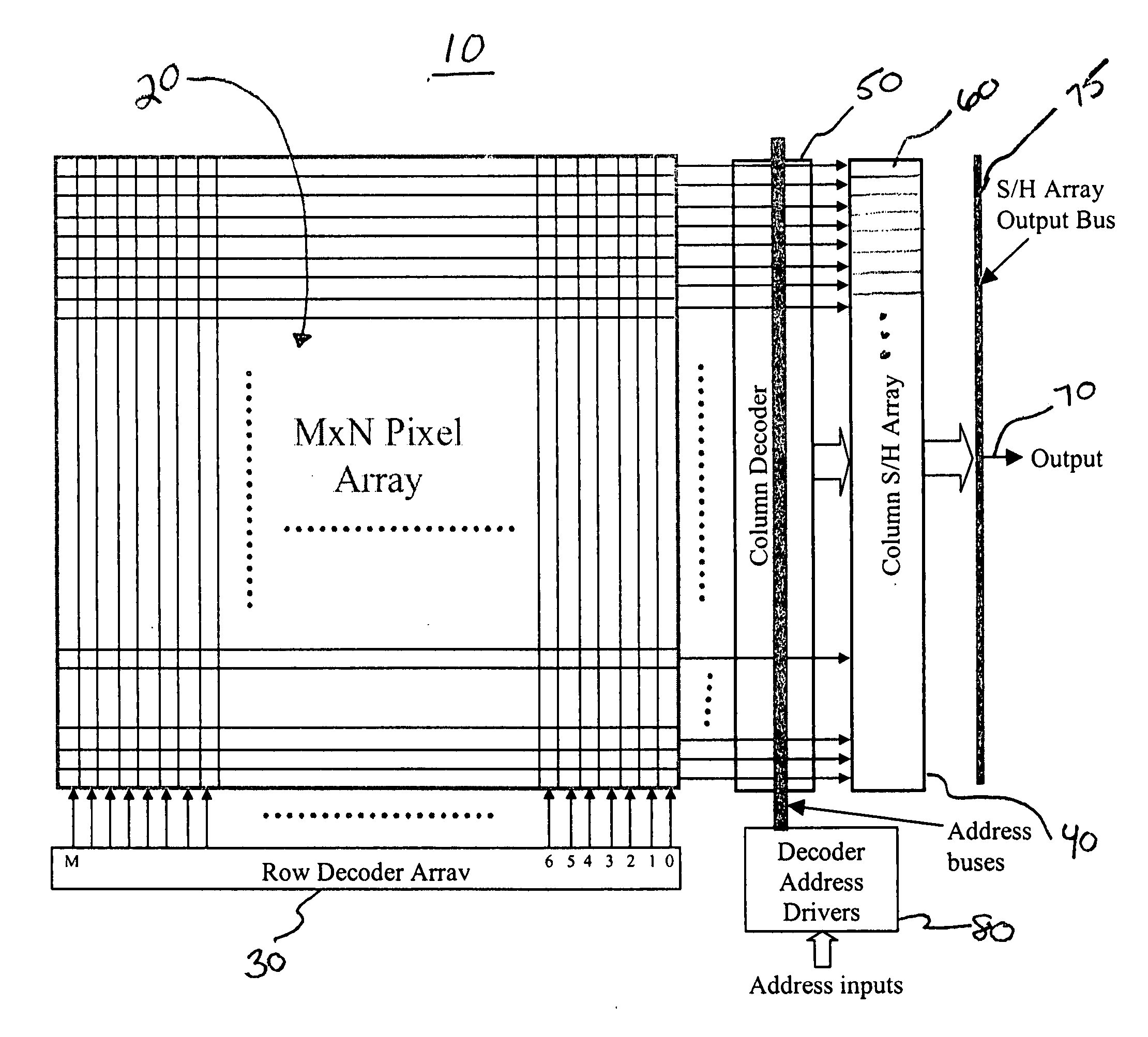
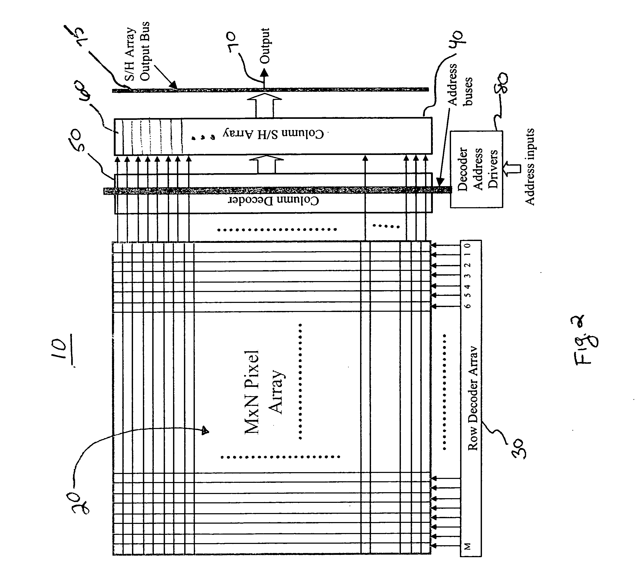
[0013] A block diagram of a CMOS image sensor 10 is shown in FIG. 2. The image sensor 10 includes a pixel array 20, a row decode...
PUM
 Abstract
Description
Claims
Application Information