

Semiconductor integrated circuit device
- Summary
- Abstract
- Description
- Claims
- Application Information
AI Technical Summary
Benefits of technology
Problems solved by technology
Method used
Image

Examples
embodiment 1
Alteration to Embodiment 1
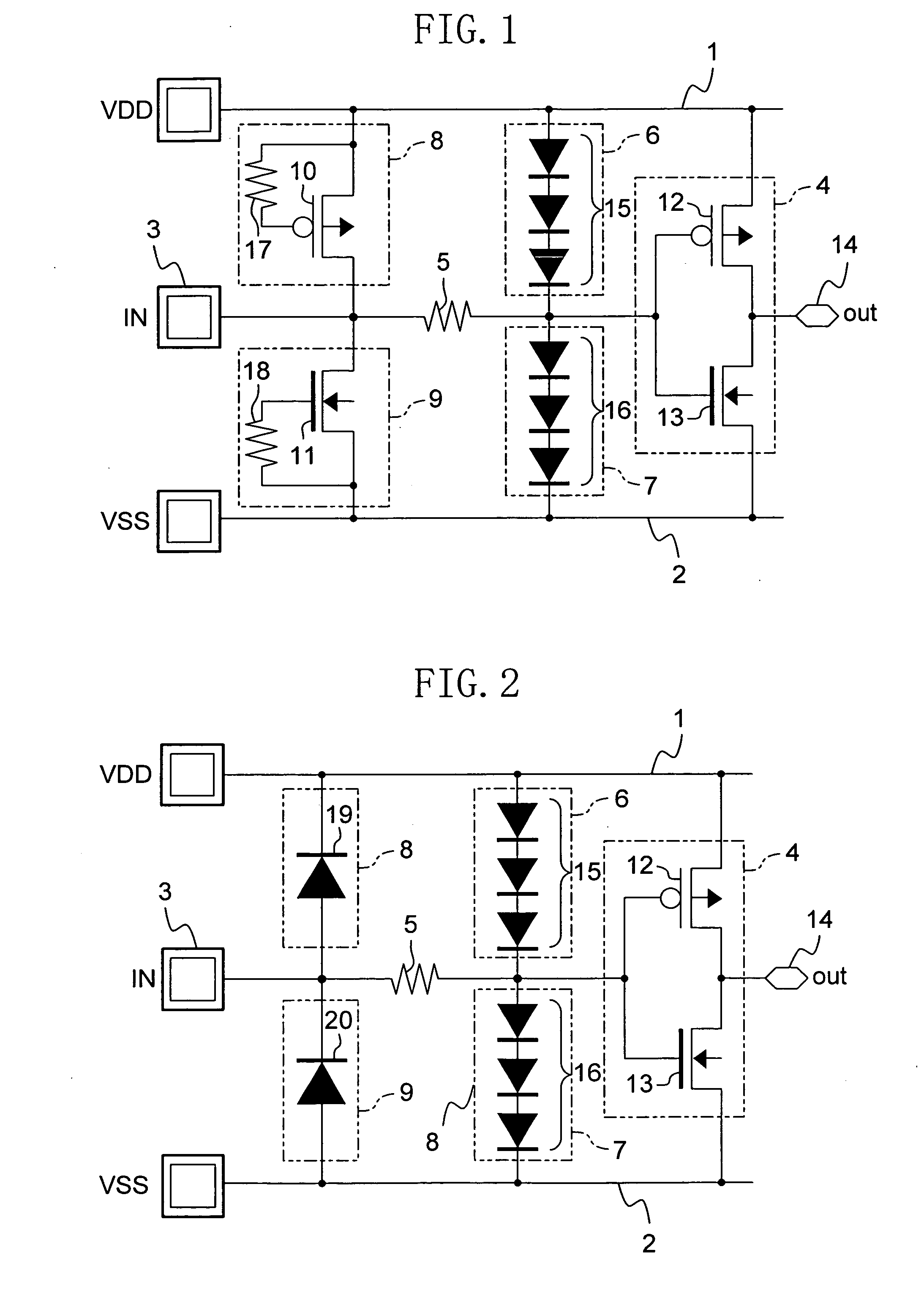
[0070]An alteration to Embodiment 1 of the present invention will be described with reference to the relevant drawing.
[0071]FIG. 2 shows a circuit configuration of a semiconductor integrated circuit device of the alteration to Embodiment 1. In FIG. 2, the same components as those shown in FIG. 1 are denoted by the same reference numerals, and the description thereof is omitted here.
[0072]As shown in FIG. 2, in the semiconductor integrated circuit device of this alteration, the third ESD protection circuit 8 is composed of a diode 19 whose cathode is connected to the power supply line 1 and whose anode is connected to the input pad 3, and the fourth ESD protection circuit 9 is composed of a diode 20 whose cathode is connected to the input pad 3 and whose anode is connected to the GND line 2.
[0073]Note herein that the diodes 19 and 20 are the same in electrical characteristics as the diodes in the first and second voltage drop circuits 15 and 16.
[0074]Hereina...
embodiment 2
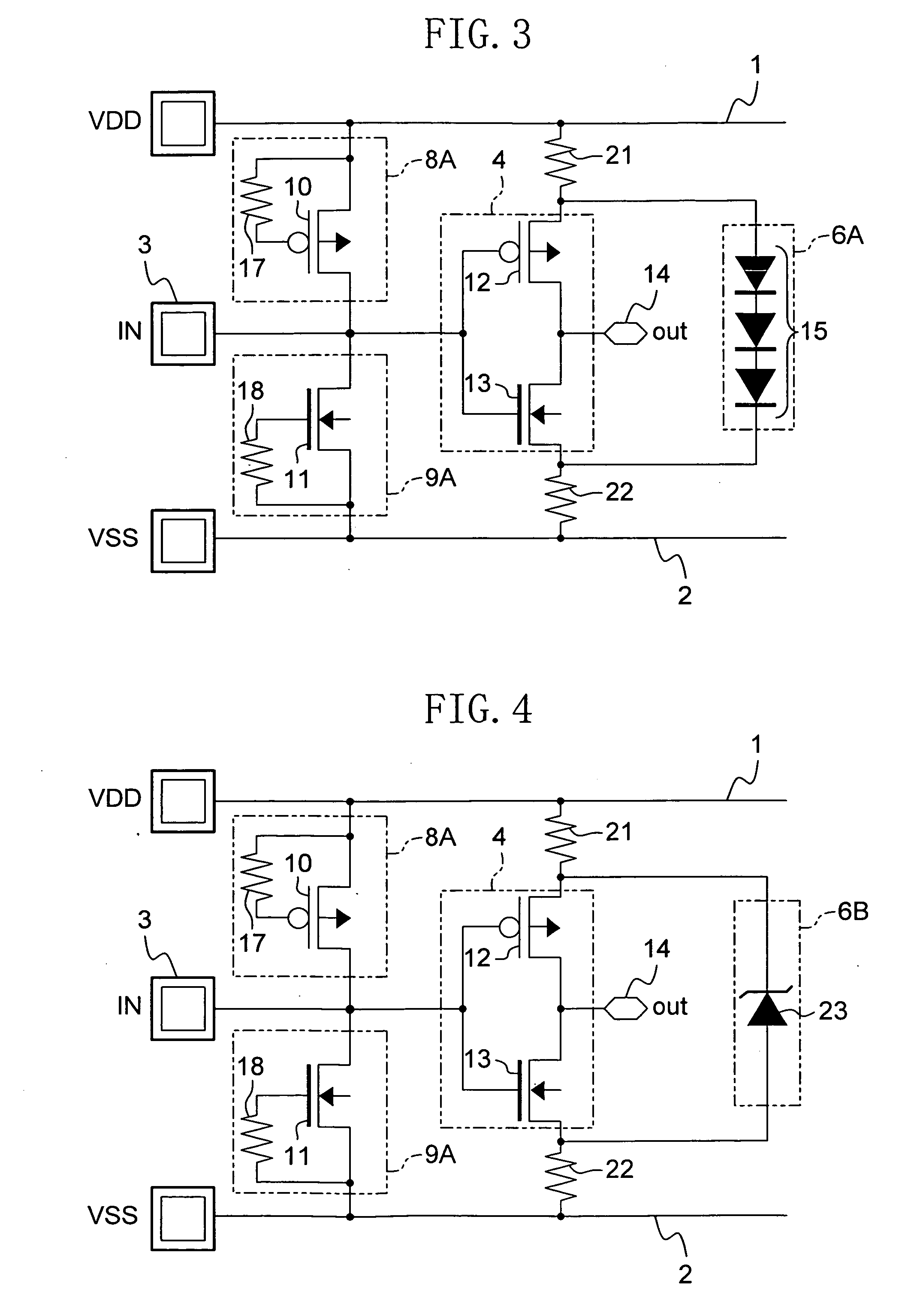
[0079]Embodiment 2 of the present invention will be described with reference to the relevant drawing.
[0080]FIG. 3 shows a circuit configuration of a semiconductor integrated circuit device of Embodiment 2 of the present invention. In FIG. 3, the same components as those shown in FIG. 1 are denoted by the same reference numerals, and the description thereof is omitted here.
[0081]As shown in FIG. 3, the semiconductor integrated circuit device of Embodiment 2 includes: an input circuit 4 connected to the input pad 3; a first ESD protection circuit 8A connected to the power supply line 1 at one terminal and to the input pad 3 at the other terminal; a second ESD protection circuit 9A connected to the input pad 3 at one terminal and to the GND line 2 at the other terminal; a first resistance 21 connected to the power supply line 1 at one terminal and to the power supply input terminal of the input circuit 4 at the other terminal; a second resistance 22 connected to the GND input terminal ...
first alteration to embodiment 2
[0093]A first alteration to Embodiment 2 of the present invention will be described with reference to the relevant drawing. FIG. 4 shows a circuit configuration of a semiconductor integrated circuit device of the first alteration to Embodiment 2. In FIG. 4, the same components as those shown in FIG. 3 are denoted by the same reference numerals, and the description thereof is omitted here.
[0094]As shown in FIG. 4, in this alteration, a Zener diode 23 is used in place of the diodes for the first voltage drop circuit constituting the third ESD protection circuit 6B.
[0095]As described above, by using the Zener diode 23 for the third ESD protection circuit 6B and setting the breakdown voltage of the Zener diode 23 at an appropriate value, it is possible to prevent occurrence of a leak current during normal operation without use of a plurality of diodes.
PUM
 Abstract
Description
Claims
Application Information