Method for forming self-aligned channel implants using a gate poly reverse mask

Inactive Publication Date: 2002-09-12
CHARTERED SEMICONDUCTOR MANUFACTURING
View PDF0 Cites 1 Cited by
  • Summary
  • Abstract
  • Description
  • Claims
  • Application Information

AI Technical Summary

Benefits of technology

[0016] It is another object of the present invention to provide a method for forming a channel implant with a lower threshhold voltage roll-off than a through the gate implant and without reverse short channel effects like a pocket implant.
[0018] The present invention provides considerable improvement over the prior art. Most importantly, the present invention provides a channel implant which can provide a lower threshhold voltage roll-off than a through the gate implant, without a reverse short channel effect as in a pocket implant. Also, the present invention can use existing photolithography reticles to form reverse gate poly masks.

Problems solved by technology

However, the implantation is difficult to control.

Method used


Image

  • Method for forming self-aligned channel implants using a gate poly reverse mask
  • Method for forming self-aligned channel implants using a gate poly reverse mask
  • Method for forming self-aligned channel implants using a gate poly reverse mask

Examples


Embodiment Construction

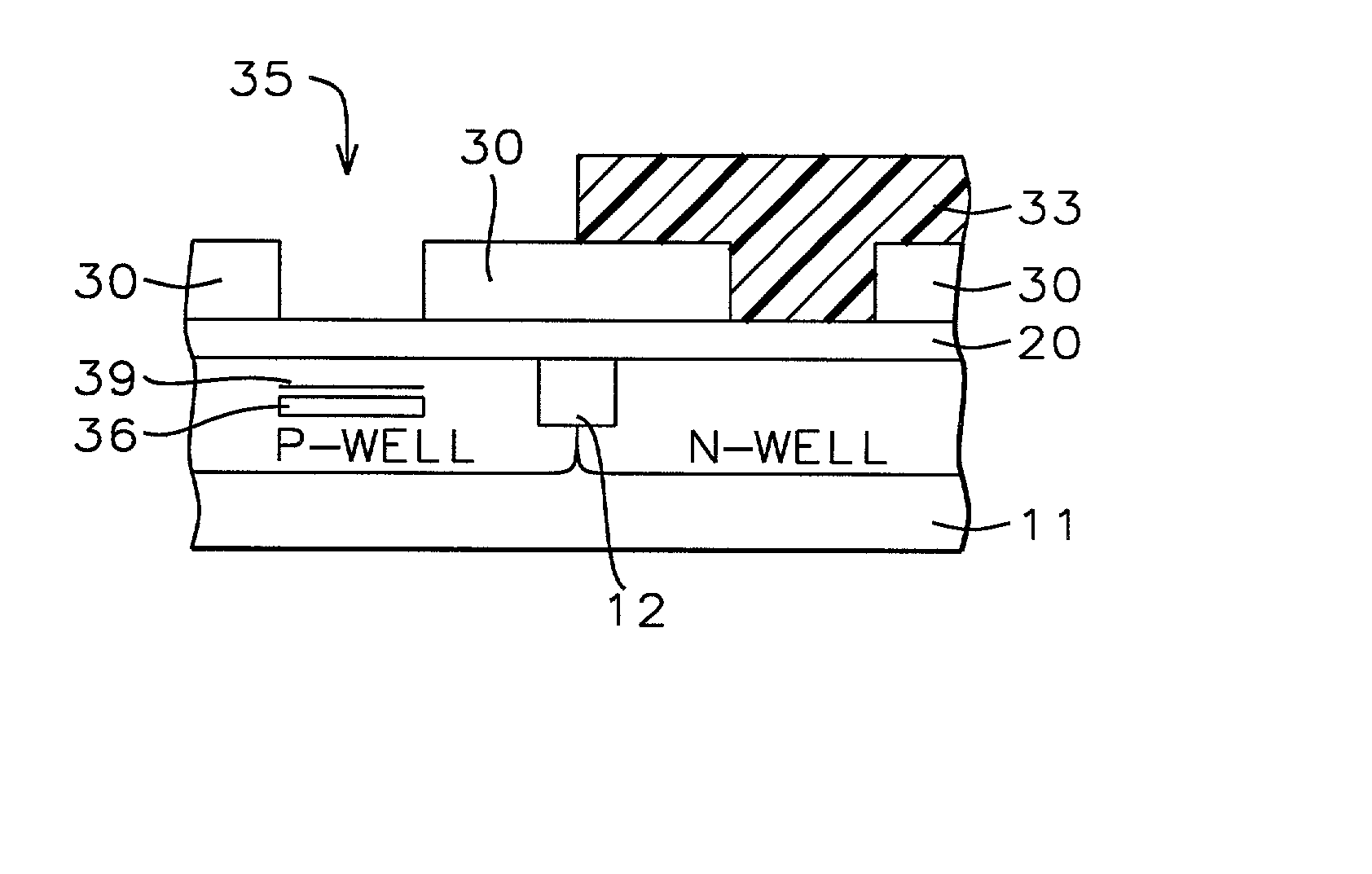
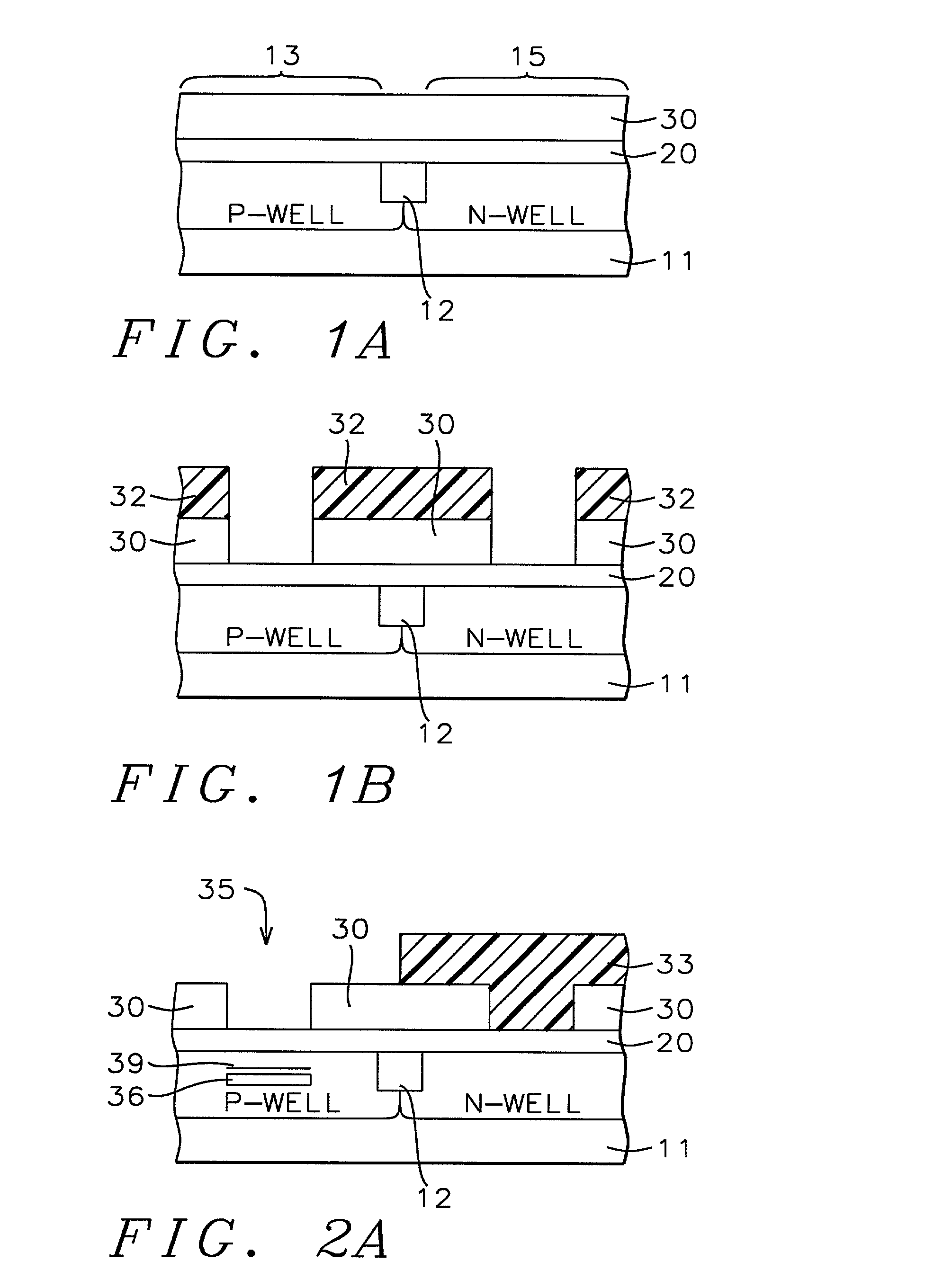
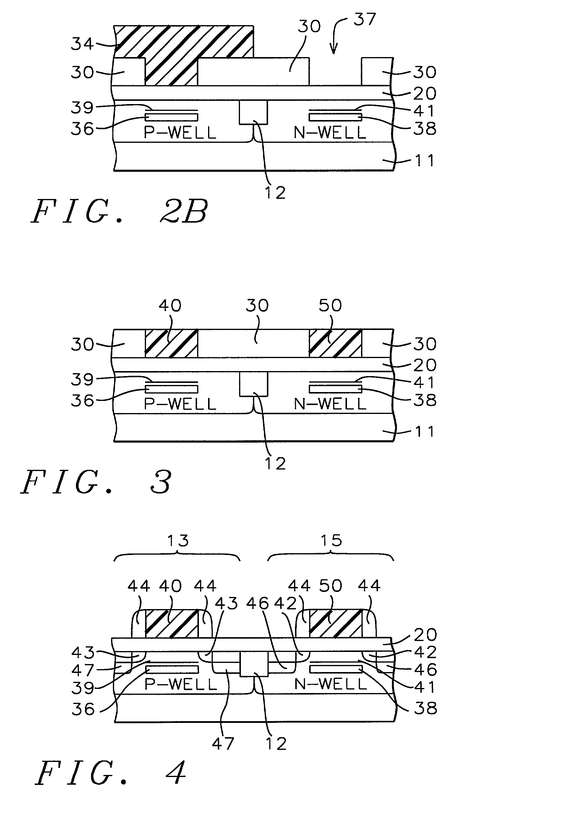
[0023] The present invention will be described in detail with reference to the accompanying drawings. The present invention provides a method for forming CMOS gates with self-aligned channel implants.

[0024] Referring to FIG. 1A, the process begins by providing a semiconductor structure (substrate) (11) having a first active area (13) and possibly having a second active area (15). The first active area (13) and the second active area (15) are defined and separated by isolation regions (12). The semiconductor substrate is understood to possibly include a wafer of semiconductor material such as monocrystalline silicon or germainium or a similar structure as is known in the art such as a silicon-on-insulator (SOI) structure. The isolation structure (12) can be any isolation structure know in the art, such as a shallow trench isolation (STI) or localized oxidation of silicon (LOCOS).

[0025] For illustrative purposes a NMOS gate will be formed in the first area (13) and a PMOS gate will be...


PUM


Abstract

A method for forming a CMOS transistor gate with a self-aligned channel implant. A semiconductor structure having a first active area is provided. A first insulating layer is formed on the semiconductor structure, and a second insulating layer is formed on the first insulating layer. The second insulating layer is patterned using a poly reverse mask and an etch selective to the first insulating layer to form a first channel implant opening, and the poly reverse mask is removed. A first channel implant mask is formed exposing the first channel implant opening. Impurity ions are implanted through the first channel implant opening to form a first threshhold adjust region and a first anti-punchthrough region. A gate layer is formed over the semiconductor structure, and the first gate layer is planarized to form a gate electrode. The second insulating layer is removed, and lightly doped source and drain regions, sidewall spacers and source and drain regions can be formed adjacent the gate electrode.

Description

BACKGROUND OF INVENTION[0001] 1) Field of the Invention[0002] This invention relates generally to fabrication of a semiconductor device and more particularly to a method for forming the self-aligned channel profile for a CMOS device using a gate poly reverse mask.[0003] 2) Description of the Prior Art[0004] The continued scaling of MOSFET gate lengths to submicron dimensions aggravates the problems of high gate resistance, polysilicon gate depletion and increased gate tunnel leakage. One method to overcome the problems of short channel effects is to use through-the-gate implantation. Channel implants are formed by implanting ions through the gate structure to form a doped region below the substrate surface in the gate area. Through-the-gate implantation can achieve the steep retrograde doping profiles, which can improve the short channel effects and increase current drivability. However, the implantation is difficult to control.[0005] Another method used is the pocket implant. A loc...

Claims


Application Information

Patent Timeline
IPC IPC(8): H01L21/8238
CPCH01L21/823807Y10S977/712
Inventor SHAO, KAIWANG, YIMINLI, JIAN XUNCHU, SHAO-FU SANFORD
Owner CHARTERED SEMICONDUCTOR MANUFACTURING
Why Eureka
Try Eureka