Semiconductor device

a technology of semiconductor devices and semiconductors, applied in the direction of organic semiconductor devices, discharge tubes/lamp details, discharge tubes luminescnet screens, etc., can solve the problem of difficult to achieve a long operating life of el elements

Inactive Publication Date: 2007-09-06
SEMICON ENERGY LAB CO LTD
View PDF5 Cites 106 Cited by
  • Summary
  • Abstract
  • Description
  • Claims
  • Application Information

AI Technical Summary

Benefits of technology

[0011] It is an object of the present invention to provide a thin-type full-color display device with the long lifetime, inexpensively, in which desired emission luminance and desired color purity can be obtained at a low voltage.
[0050] According to the present invention, a thin-type full-color display device with the long lifetime, in which desired emission luminance and desired color purity can be obtained at a low voltage, can be provided inexpensively.

Problems solved by technology

Therefore, it is difficult to achieve a long operating life of the EL element on a condition that light-emitting elements of a red color, a green color, or a blue color all have the same luminance and be driven at a low voltage.

Method used


Image

  • Semiconductor device
  • Semiconductor device
  • Semiconductor device

Examples


embodiment mode 1

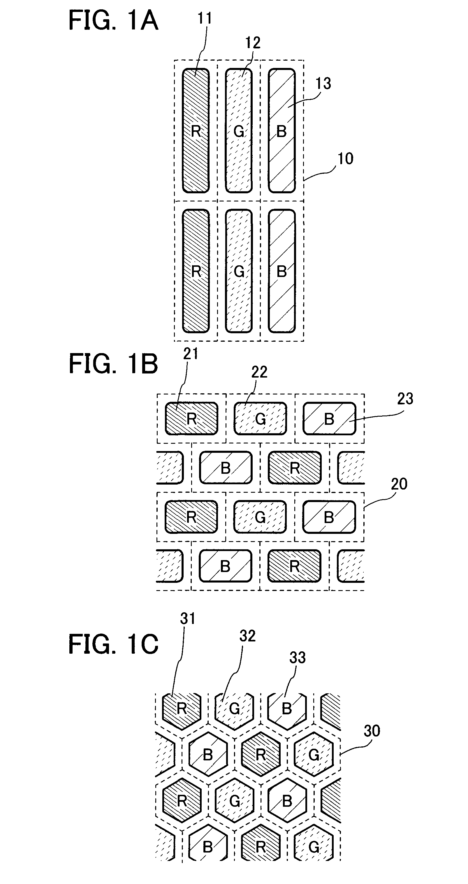
[0066] A full-color display device relating to Embodiment Mode 1 of the present invention will be explained with reference to FIG. 1A, FIGS. 2A to 2C, FIGS. 3A to 3C, FIG. 4, and FIG. 5.

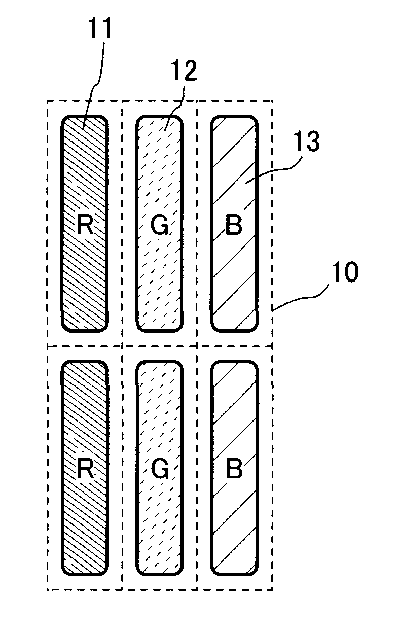
[0067]FIG. 1A shows a top view of part of a pixel for performing full-color display by three-color driving of RGB. In FIG. 1A, a region surrounded by a dot line is a pixel region 10, where an organic material layer 11, an organic material layer 12, and an inorganic material layer 13, each of which is to be a light-emitting layer (or a fluorescent layer) of a light-emitting element, are formed with intervals so as not to be overlapped with each other.

[0068] Each of the organic material layer 11, the organic material layer 12, and the inorganic material layer 13 is interposed between a pair of electrodes, whereby three light-emitting elements are formed. When a voltage is applied between the pair of electrodes of each light-emitting element, the light-emitting elements each emit light of a red color,...

embodiment mode 2

[0097] In this embodiment mode, an example of a delta-type pixel arrangement is shown in FIG. 1B, in which an interval between pixels adjacent to each other can be narrowed.

[0098] In a pixel structure of this embodiment mode, an inorganic EL element emitting green light is used, which has a different emission color from that of the inorganic EL element in Embodiment Mode 1. This embodiment mode shows an example of performing full-color display by a pixel structure in which an inorganic EL element emitting green light, an organic EL element emitting blue light, and an organic EL element emitting red light are used.

[0099] In FIG. 1B, a region surrounded by a dot line is a pixel region 20 where an organic material layer 21, an inorganic material layer 22, and an organic material layer 23, each of which is to be a light-emitting layer (or a fluorescent layer) of a light-emitting element, are formed with keeping intervals so as not to be overlapped with each other.

[0100] Here, as the ...

embodiment mode 3

[0108] In this embodiment mode, an example of arrangement of a light-emitting element will be shown in FIG. 1C, in which a shape of a light-emitting region is not rectangle but hexagon.

[0109] In a pixel structure of this embodiment mode, an inorganic EL element emitting red light is used, which has a different emission color from that of the inorganic EL element in Embodiment Mode 1. This embodiment mode shows an example of performing full-color display by a pixel structure in which this inorganic EL element emitting red light, an organic EL element emitting blue light, and an organic EL element emitting green light are used.

[0110] In FIG. 1C, a region surrounded by a dot line is a pixel region 30 where an inorganic material layer 31, an organic material layer 32, and an organic material layer 33, each of which is to be a light-emitting layer (or a fluorescent layer) of a light-emitting element, are formed with keeping intervals so as not to be overlapped with each other.

[0111] H...


PUM


Abstract

It is an object to provide a thin-type full-color display device with the long lifetime, inexpensively, in which desired emission luminance and desired color purity can be obtained at a low voltage. In a light-emitting device capable of full-color display, among a plurality of light-emitting elements emitting different emission colors (for example, colors of red (R), green (G), and blue (B)), at least one of the light-emitting elements of an emission color is a light-emitting element including an organic compound (an organic EL element), and the other light-emitting element of an emission color is a light-emitting element using an inorganic material as a light-emitting layer or a fluorescent layer (an inorganic EL element). It is to be noted that the organic EL element and the inorganic EL element are formed over the same substrate.

Description

BACKGROUND OF THE INVENTION [0001] 1. Field of the Invention [0002] The present invention relates to a semiconductor device including a plurality of light-emitting elements and a manufacturing method thereof. For example, the present invention relates to an electronic device that mounts a light-emitting display device including a light-emitting element as a component. [0003] It is to be noted that a semiconductor device in the present specification generally indicates a device capable of functioning by utilizing semiconductor characteristics, and electro-optic devices, semiconductor circuits, and electronic devices are all semiconductor devices. [0004] 2. Description of the Related Art [0005] A phenomenon in which light emission is generated when applying an electric field to a substance is referred to as an EL (Electroluminescence) phenomenon, which is a known phenomenon. An inorganic EL using an inorganic thin film of ZnS:Mn and an organic EL using an organic evaporation thin film...

Claims


Application Information

Patent Timeline
Patent Type & Authority Applications(United States)
IPC IPC(8): H01L27/32
CPCH01L27/286H01L27/3211H01L27/3213H01L27/322H01L2251/5323H01L27/3244H01L27/3281H01L2251/5315H01L27/3225H10K19/20H10K59/351H10K59/00H10K59/38H10K59/17H10K59/12H10K2102/3026H10K2102/3031H05B33/14
Inventor YAMAZAKI, SHUNPEISAKATA, JUNICHIROAOYAMA, TOMOYAOHSHIMA, KOHEIMATSUBARA, RIEKUWABARA, HIDEAKI
Owner SEMICON ENERGY LAB CO LTD
Why Eureka
Try Eureka