Method and apparatus of time and space co-divided atomic layer deposition

a technology time-space division, applied in the field of atomic layer deposition apparatuses and methods, can solve the problems of significant downtime, difficult application of cvd and pvd methods in high-throughput operations, and insufficient performance of conventional cvd and pvd methods in forming uniform thin films over substrates with high aspect ratio features

Inactive Publication Date: 2007-09-20
ASM GENITECH KOREA
View PDF22 Cites 174 Cited by
  • Summary
  • Abstract
  • Description
  • Claims
  • Application Information

AI Technical Summary

Benefits of technology

[0016] In yet another embodiment of the invention, vapor phase deposition apparatuses are provided. The apparatuses comprise a plurality of spatially-separated reaction zones including a first reaction zone and a second reaction zone, each of the reaction zones communicating with a gas source, each of the reaction zones comprising an axis perpendicular to an opening in each of the reaction zones, each opening configured to accept a substrate...

Problems solved by technology

Unfortunately, conventional CVD and PVD methods do not perform satisfactorily in forming uniform thin films over substrates including high aspect-ratio features, such as vias and trenches.
The self-limiting nature of ALD makes its application in high-throughput operations difficult since formation of films or thin fi...

Method used


Image

  • Method and apparatus of time and space co-divided atomic layer deposition
  • Method and apparatus of time and space co-divided atomic layer deposition
  • Method and apparatus of time and space co-divided atomic layer deposition

Examples


Embodiment Construction

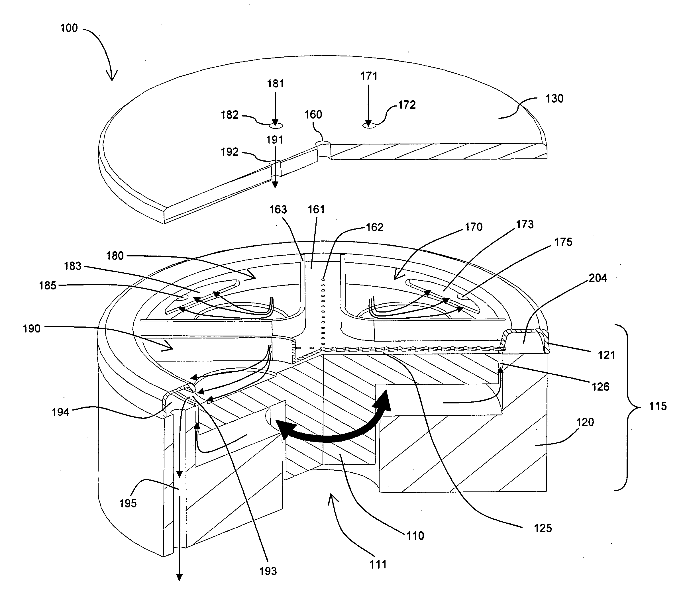
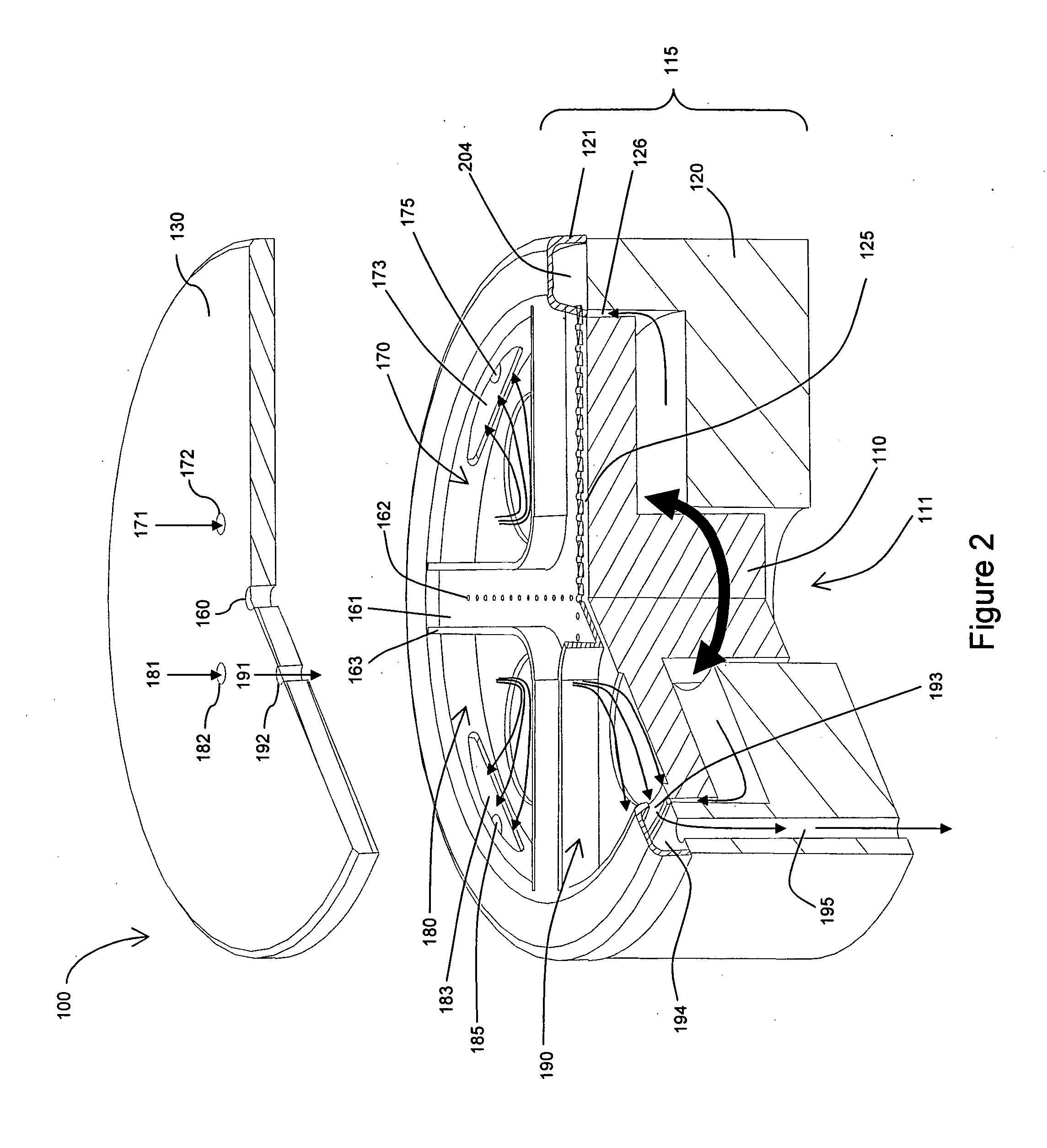
[0029] The inventors have observed several problems associated with prior art multi-wafer ALD systems. For example, in systems employing the space separation method, variation of pulsing times (variable pulsing frequency) between reaction spaces is not possible. As another example, in systems employing the space separation method, moving parts supporting wafers are also contacted with reactant gases. Film deposition occurs on the wafer supporting moving parts as well as wafer surfaces, leading to problems associated with particle generation. This is particularly problematic in systems configured for in situ (or direct) plasma generation using an RF electrode placed in the reaction space, in which metallic film deposition on reactor walls may lead to electrical shorting between the walls of the reactor and the RF electrode. This may significantly impede, even prevent, plasma generation.

[0030] Preferred embodiments of the present invention resolve the problems and shortcomings associ...


PUM

PropertyMeasurementUnit
Timeaaaaaaaaaa
Pressureaaaaaaaaaa
Flow rateaaaaaaaaaa

Abstract

Space and time co-divided atomic layer deposition (ALD) apparatuses and methods are provided. Substrates are moved (e.g., rotated) among multiple reaction zones, each of which is exposed to only one ALD reactant. At the same time, reactants are pulsed in each reaction zone, with purging or other gas removal methods between pulses. Separate exhaust passages for each reactant and purging during wafer movement minimizes particle contamination. Additionally, preferred embodiments permit different pulsing times in each reaction space, thus permitting flexibility in pulsing.

Description

BACKGROUND OF THE INVENTION [0001] 1. Field of the Invention [0002] The invention generally relates to semiconductor processing and, more particularly, to atomic layer deposition (ALD) apparatuses and methods. [0003] 2. Description of the Related Art [0004] As semiconductor integration technologies advance, process methods for depositing a thin film uniformly and conformally become increasingly important. Here, the thin film may be an insulator or a conductor. Thin film deposition methods are largely categorized into three types: chemical vapor deposition (CVD), physical vapor deposition (PVD) and atomic layer deposition (ALD), sometimes called atomic layer epitaxy (ALE). [0005] In CVD, gas phase materials generally react on the top surface of a substrate heated to a temperature between about 100° C. to 1,000° C., whereby a solid material produced as a result of such reaction is deposited on the top surface of the substrate. In PVD, films are typically deposited onto a substrate sur...

Claims


Application Information

Patent Timeline
IPC IPC(8): C30B23/00C23C16/00
CPCC23C16/45551C23C16/4584C23C16/45527
Inventor PARK, HYUNG-SANGTAK, YOUNG-DUCKKOH, WONYONGSHIMIZU, AKIRA
Owner ASM GENITECH KOREA
Why Eureka
Try Eureka