

Thin film transistor device with high symmetry
- Summary
- Abstract
- Description
- Claims
- Application Information
AI Technical Summary
Benefits of technology
Problems solved by technology
Method used
Image

Examples
Embodiment Construction
[0019]For your esteemed members of reviewing committee to further m understand and recognize the fulfilled functions and structural characteristics of the invention, several preferable embodiments cooperating with detailed description are presented as the follows.
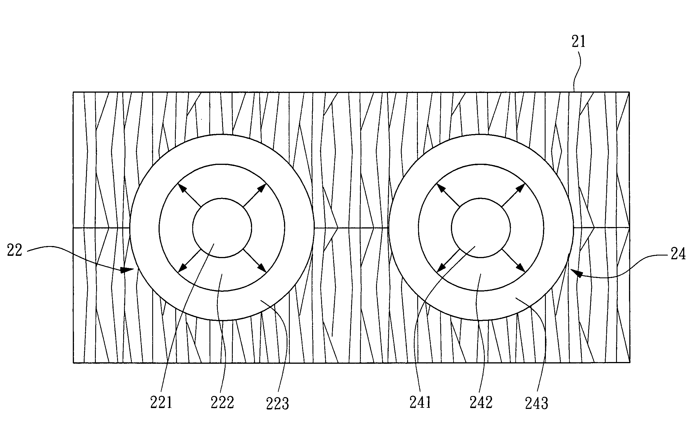
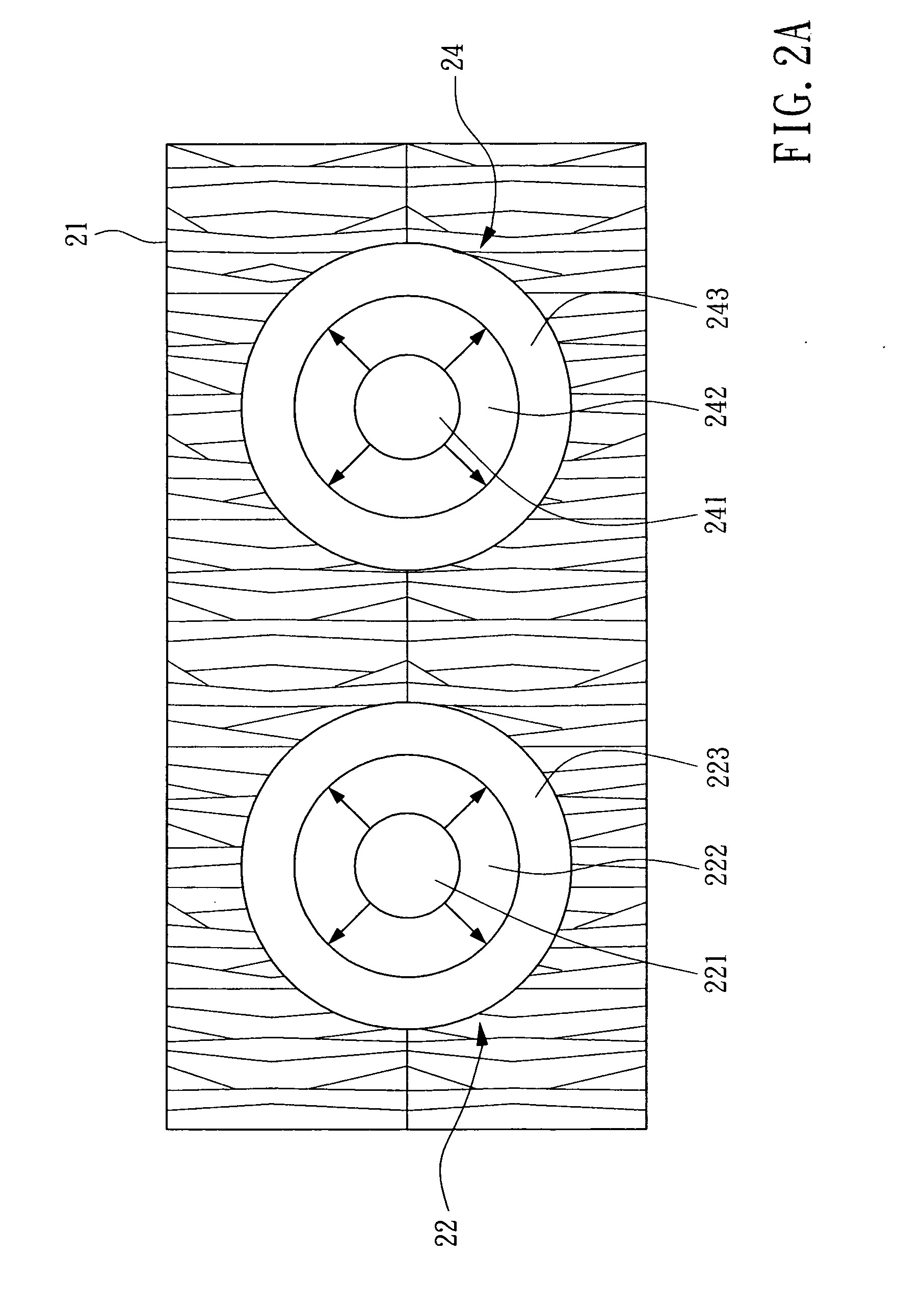
[0020]During the manufacturing of a thin film transistor device with high symmetry according to a preferred embodiment of the invention, a layer of amorphous silicon (a-Si) film is first being deposited on a glass or quartz substrate by a means of sputtering or low pressure chemical vapor deposition (LP-CVD); and then the a-Si film is converted into a polycrystalline silicon film by a means of sequential lateral solidification (SLS) for growing silicon grains following a single direction.
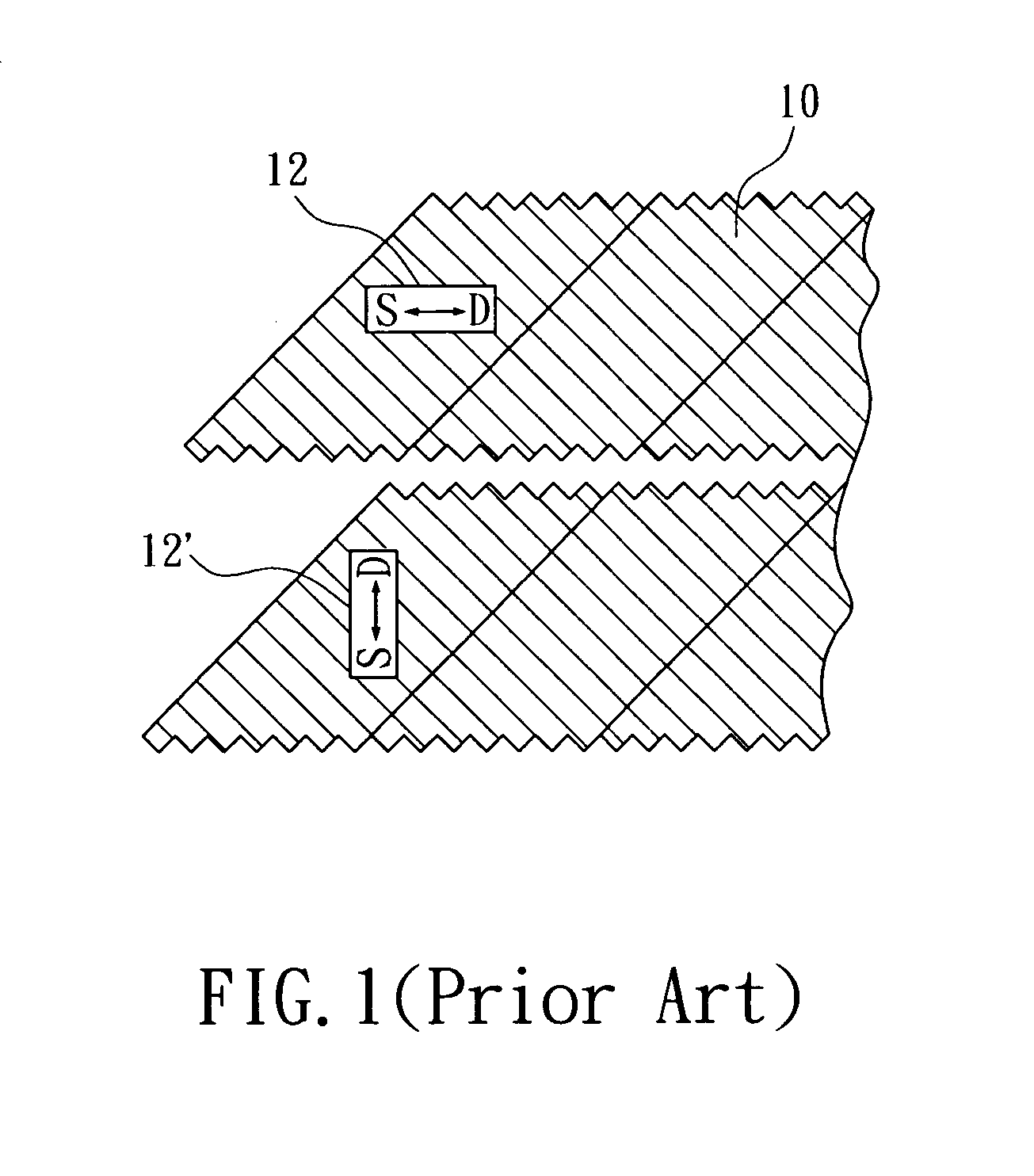
[0021]As those disclosed in prior art, if the channel directions of the TFT devices of an LCD device formed on the SLS-crystallized silicon film are different to each other, that is, some TFTs are formed with channel directions parallel to ...
PUM
 Abstract
Description
Claims
Application Information