
Defect inspecting apparatus

Inactive Publication Date: 2007-09-20
HITACHI HIGH-TECH CORP
View PDF5 Cites 11 Cited by
  • Summary
  • Abstract
  • Description
  • Claims
  • Application Information

AI Technical Summary

Benefits of technology

[0018]As described above, the invention enables highly-sensitive detection of a defect wherein focal depth becomes shallow while stabilizing the sensitivity without lowering of the operating rate by calibration.
[0020]When the invention is applied, a thermostatic chamber is not required as measures for change in temperature, and therefore a size, cost and requirement for environment of equipment can be reduced.

Problems solved by technology

In the cases of JP-A-63-135848, No. 1-117024 and No. 2000-105203, the defect detection sensitivity fluctuates owing to changes in temperature or barometric pressure at a location where the defect inspecting apparatus is installed and sensitivity calibration frequency tends to increase due to the following reasons, improving deterioration in an operating rate of the apparatus due to frequent calibration is a challenge.
A clean room in which a defect inspecting apparatus is installed often provides an insufficient distance from adjacent equipment or a wall, and a local temperature in the environment of installation may change in about an hour.
Keeping the detection sensitivity needs sensitivity calibration, but more frequent calibration may lower the operating rate of the apparatus because one calibration requires several minutes.
For measures against it, there is a method of installing an apparatus in a dedicated thermal chamber, but because of disadvantages that the apparatus may be expensive and a footprint may be enlarged, this method is not suitable for a defect inspecting apparatus.
Further, on the one hand, because barometric pressure in a clean room is not controlled, the sensitivity may become unstable when a low or high atmospheric pressure passes.

Method used


Image

  • Defect inspecting apparatus
  • Defect inspecting apparatus
  • Defect inspecting apparatus

Examples


Embodiment Construction

[0034]Embodiments of the invention will be described hereinafter with reference to the drawings. In the following drawings, similar functional portions are denoted by the same reference signs.

[0035]First, a substrate 1 to be inspected for a defect such as a particle etc. according to the invention will be described with reference to FIGS. 7 and 8. Since the details are described in Japanese Patent No. 3566589, the summary will be provided.

[0036]The substrate 1 to be inspected for a defect such as a particle etc. may be, as shown in FIG. 7, a semiconductor wafer 1a on which chips 1aa comprised of memory LSIs are arrayed two-dimensionally at predetermined intervals. The chip 1aa comprised of the memory LSI is mainly formed with a memory cell region 1ab, a peripheral circuit region 1ac comprised of a decoder, a control circuit and the like, and another region 1ad. The memory cell region 1ab is formed by arraying (repeatedly) a memory cell pattern two-dimensionally and regularly. Howeve...


PUM


Abstract

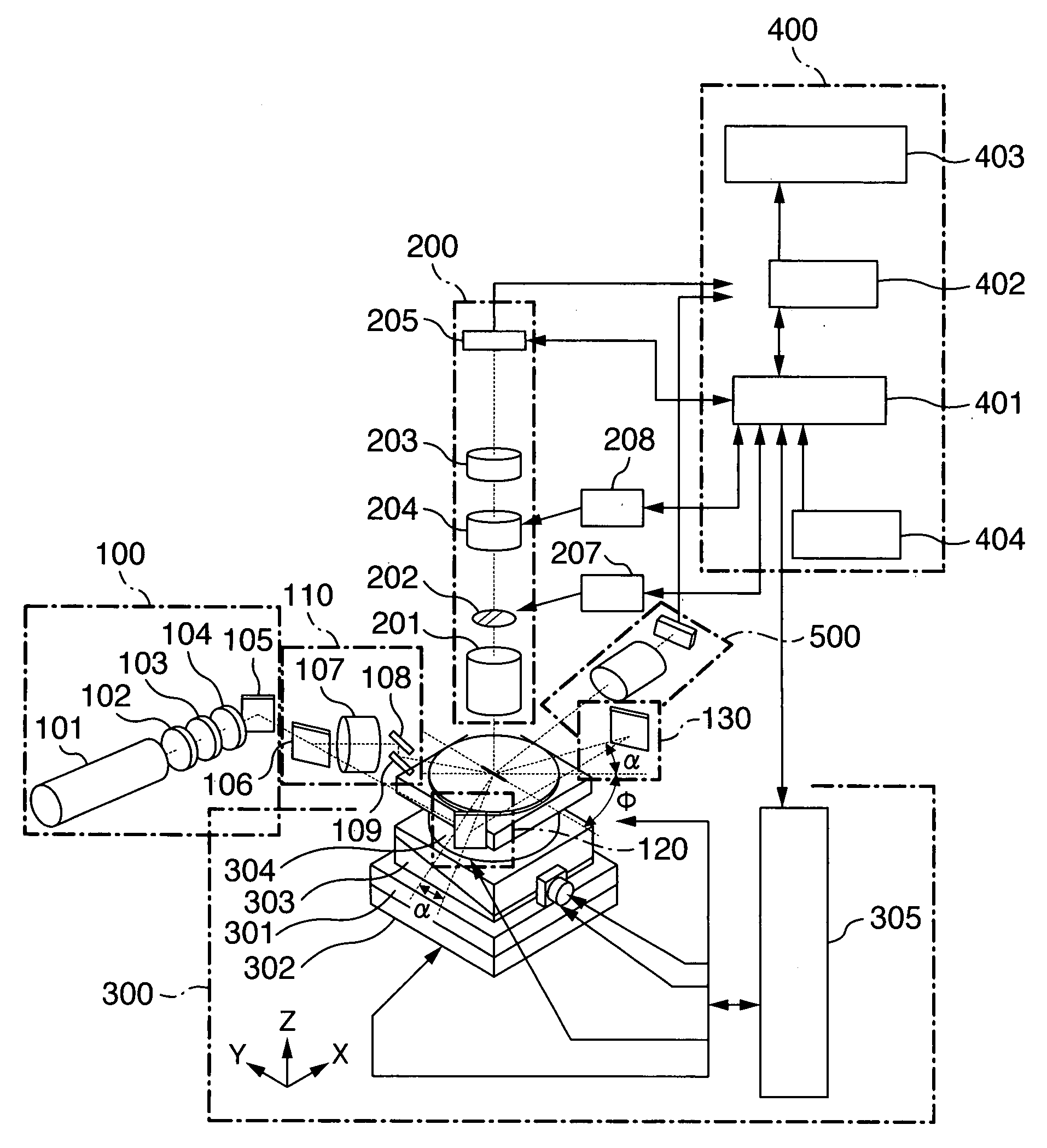
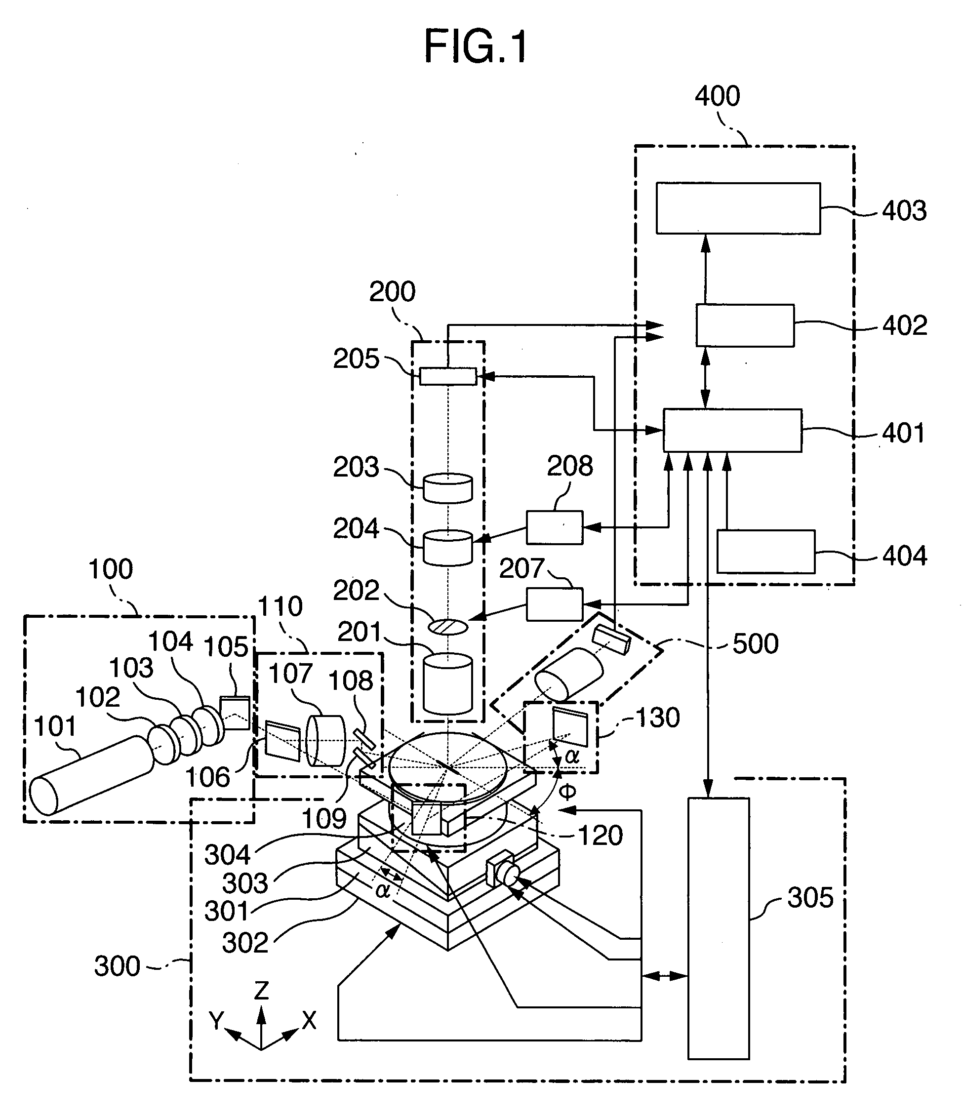
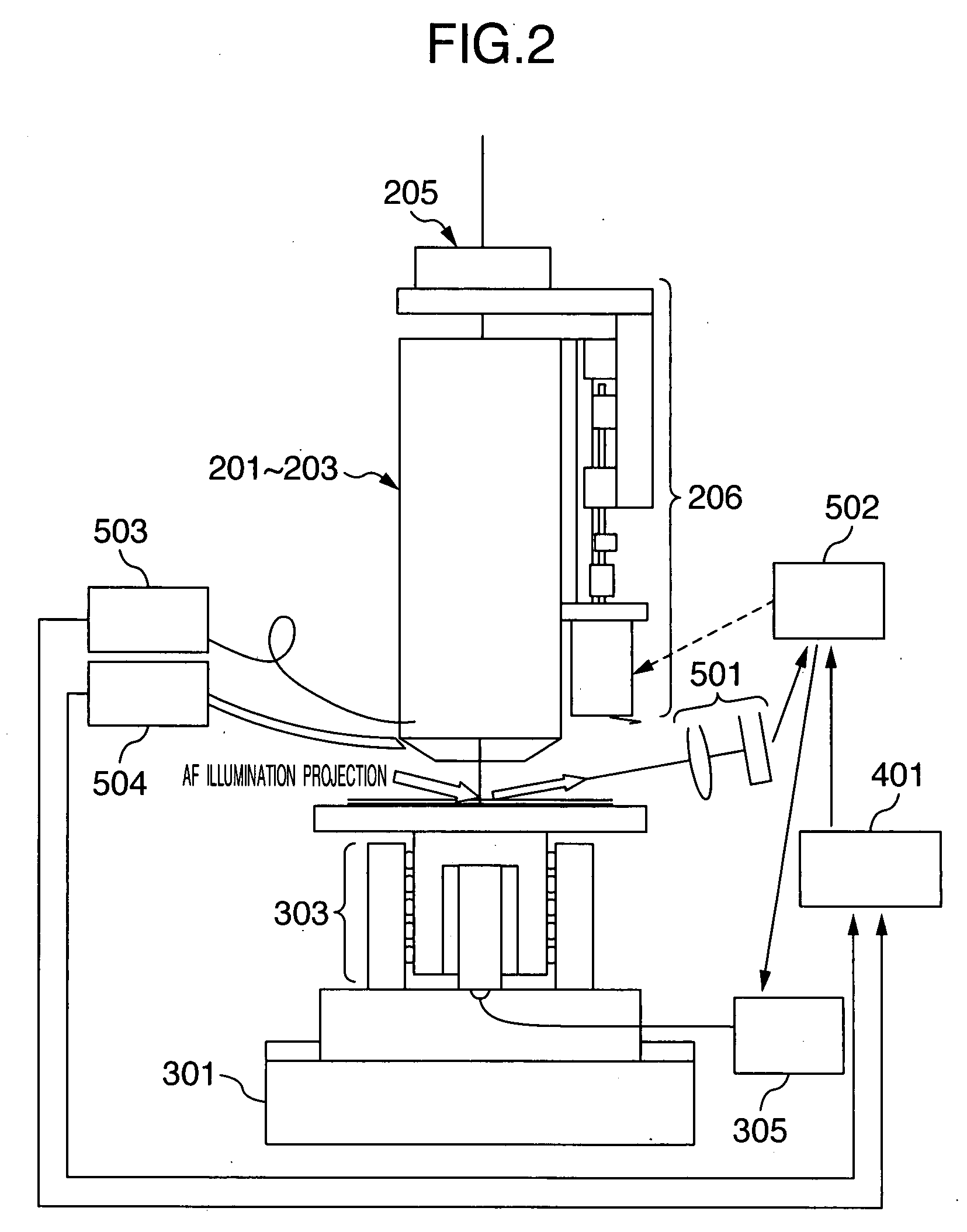
A defect inspecting apparatus of the invention solves a problem that in a defect inspecting apparatus, because of improving detection sensitivity of a microscopic defect by reducing a detection pixel size, a focal depth becomes shallow, a height of imaging is varied due to environmental change and the detection sensitivity of a defect becomes unstable. This apparatus comprises an XY stage, which carries a substrate to be inspected and scans in a predetermined direction, and a mechanism having a system of irradiating a defect on the inspected substrate at a slant and detecting the defect by a detection optical system disposed on the upper side, which corrects a height of imaging in real time for change in temperature and barometric pressure in order to keep the imaging in a best condition.

Description

BACKGROUND OF THE INVENTION [0001]The present invention relates to an inspection method and inspecting apparatus, particularly to a technology suitable for inspecting the generation state of a defect such as a particle etc. in a manufacturing process by inspecting a defect such as a particle etc. produced in the manufacturing process for forming a pattern on a substrate to manufacture an object, such as a semiconductor manufacturing process, a liquid display element manufacturing process, and a printed circuit board manufacturing process, analyzing and taking measures.[0002]In a semiconductor manufacturing process, a particle on a semiconductor substrate (wafer) may cause a failure such as an insulation failure or shot-circuit. Further, as semiconductor elements become miniaturized, if a microscopic particle is present, the microscopic particle may cause an insulation failure of a capacitor or breakdown of a gate oxide film. Such a particle comes to be mixed in, with taking various ...

Claims


Application Information

Patent Timeline
IPC IPC(8): G01N21/88
CPCG01N21/94G01N21/9501G01N2201/1218G01N2201/1211G01N2021/8822
Inventor CHIKAMATSU, SHUICHINOGUCHI, MINORIAIKO, KENJI
Owner HITACHI HIGH-TECH CORP
Learn More