Capacitance-compensated differential circuit line layout structure

a differential circuit line and layout structure technology, applied in the field of circuit layout technology, can solve the problems of receiving a weak signal, difficult and tedious layout work of wave-shaped microstrip segments, and difficult implementation of current computer-aided circuit layout drawing programs, and achieve the effect of simplifying the layout work of differential circuit lines and being easy to implemen

Inactive Publication Date: 2007-09-27
LAI CHUN YU
View PDF4 Cites 9 Cited by
  • Summary
  • Abstract
  • Description
  • Claims
  • Application Information

AI Technical Summary

Benefits of technology

[0012] Structurally, the capacitance-compensated differential circuit line layout structure according to the invention comprises: (A) a pair of differential circuit lines, including a first circuit line and a second circuit line, which extend over the circuit board in a curved path and thus include at least one bent portion, wherein the first circuit line is laid radially inside the second circuit line at each bent portion; and (B) at least one branched electrically-conductive pad, which is laid beside the bent portion of the first circuit line and electrically connected to the first circuit line for providing an equivalent capacitive effect to the first circuit line.
[0013] The capacitance-compensated diffe...

Problems solved by technology

One drawback to the provision of the above-mentioned wave-shaped microstrip segments 130, however, is that the wave-shaped microstrip segments 130 each include a series of U-shaped segments which would undesirably cause discontinuity in the transmission of the UHF digital signal over the first circuit line 110, thus resulting in signal reflections that would cause the processing circuitry (not shown) at the terminal point B to receive a weakened signal.
Still one drawback to the utilization of the above-mentioned wave-...

Method used


Image

  • Capacitance-compensated differential circuit line layout structure
  • Capacitance-compensated differential circuit line layout structure
  • Capacitance-compensated differential circuit line layout structure

Examples


Embodiment Construction

[0020] The capacitance-compensated differential circuit line layout structure according to the invention is disclosed in full details by way of preferred embodiment in the following with reference to FIG. 2 through FIG. 5.

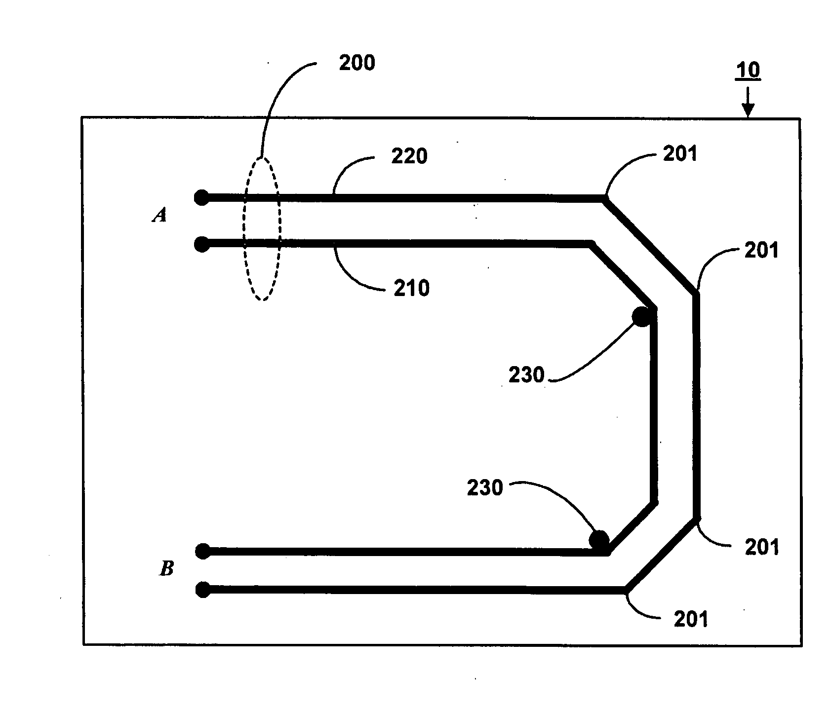
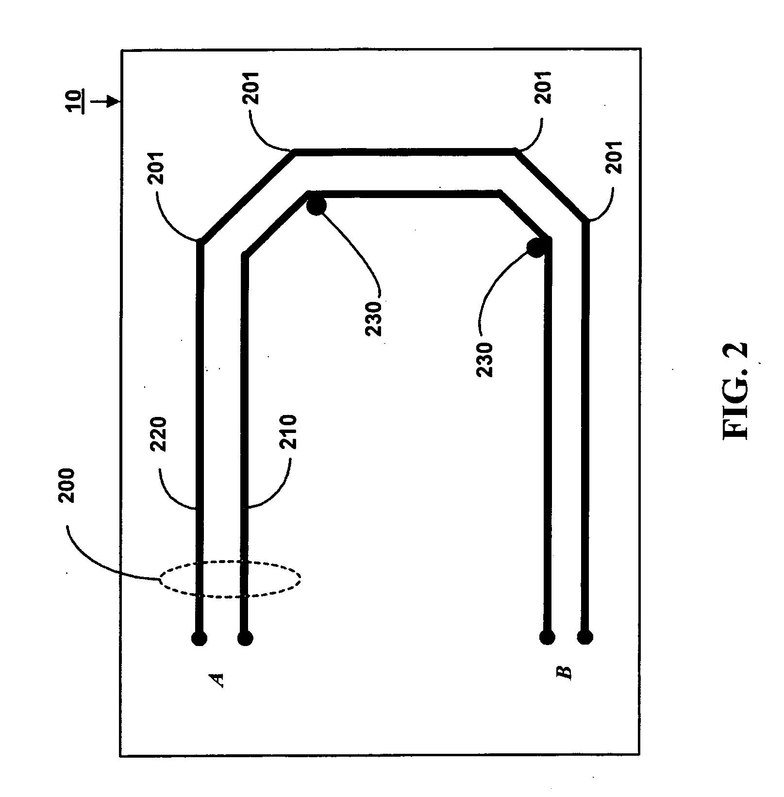
[0021]FIG. 2 is a schematic diagram showing a preferred embodiment of the capacitance-compensated differential circuit line layout structure 200 according to the invention. As shown, the capacitance-compensated differential circuit line layout structure 200 of the invention comprises: (A) a pair of circuit lines, including a first circuit line 210 and a second circuit line 220; and (B) at least one branched electrically-conductive pad 230.

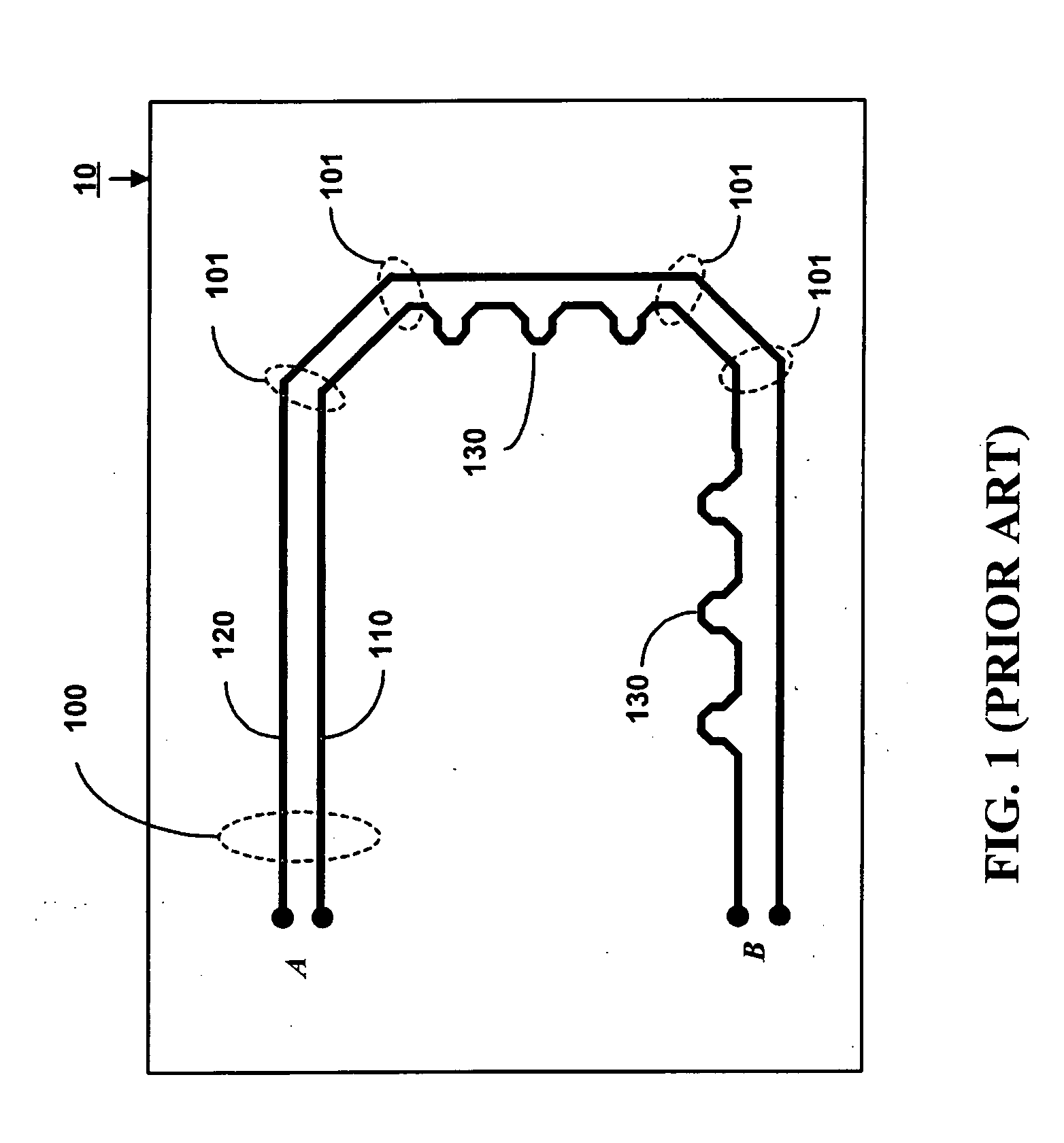
[0022] The first circuit line 210 and the second circuit line 220 are, for example, a pair of microstrips used for the transmission of ultra-high frequency signals, such as a pair of differential UHF digital signals, and which are separated by a predetermined distance and extend over the circuit board 10 along a curved path. Str...


PUM


Abstract

A capacitance-compensated differential circuit line layout structure is proposed, which is designed for use on a circuit board, such as a high-speed digital circuit board, for the layout of a pair of differential circuit lines on the high-speed digital circuit board, and which is characterized by the provision of a branched electrically-conductive pad at the bent portion of the radially-side one of the two differential circuit lines (i.e., the shorter one of the two circuit lines), for the purpose of providing the shorter one of the circuit lines with a capacitive effect that can cause a time delay to the ultra-high frequency digital signal passing therethrough, thereby eliminating the undesired effects of phase skew and signal reflection. In addition, this feature also allows the layout work of the differential pair of circuit lines to be more simplified and thus easier to implement than the prior art.

Description

BACKGROUND OF THE INVENTION [0001] 1. Field of the Invention [0002] This invention relates to circuit layout technology, and more particularly, to a capacitance-compensated differential circuit line layout structure which is designed for use on a circuit board, such as a high-speed digital circuit board, for the layout of a pair of differential circuit lines on the high-speed digital circuit board. [0003] 2. Description of Related Art [0004] With the advent of wireless digital communication technologies, such as wireless networking, mobile phones, GPS (Global Positioning System), etc., the design and manufacture of high-speed digital circuit boards that handle digital signals in the gigahertz range is in high demand in the electronics industry. In circuit layout design, high-speed digital circuit boards typically use microstrips for transmission of digital signals at ultra-high frequencies (UHF), typically in the range from 1 GHz to 3 GHz (gigahertz). [0005] In the design of high-sp...

Claims


Application Information

Patent Timeline
IPC IPC(8): H01P3/00
CPCH01P3/081H05K1/0245H05K2201/09272H05K2201/09236H05K2201/09263H05K1/0248
Inventor LAI, CHUN-YU
Owner LAI CHUN YU
Why Eureka
Try Eureka