Functional device

a functional device and device technology, applied in the direction of thermoelectric devices, organic semiconductor devices, solid-state devices, etc., can solve the problems of complex device structure, low emission intensity, and inability to obtain uniform luminance, and achieve excellent production suitability and uniform in-plane output.

Active Publication Date: 2007-10-04
UDC IRELAND
View PDF21 Cites 22 Cited by
  • Summary
  • Abstract
  • Description
  • Claims
  • Application Information

AI Technical Summary

Benefits of technology

[0019]According to the invention, provided is an improved functional device which is excellent in production suitability and can give a uniform in-plane output.

Problems solved by technology

However, as the distance from the electrode terminal increases, a more voltage drop is caused so that the emission intensity becomes lower.
Thus, the device has a problem that uniform luminance cannot be obtained.
However, any of these attempts makes the device structure thereof complicated, and is insufficient in practical device production suitability.

Method used


Image

  • Functional device
  • Functional device
  • Functional device

Examples


first embodiment

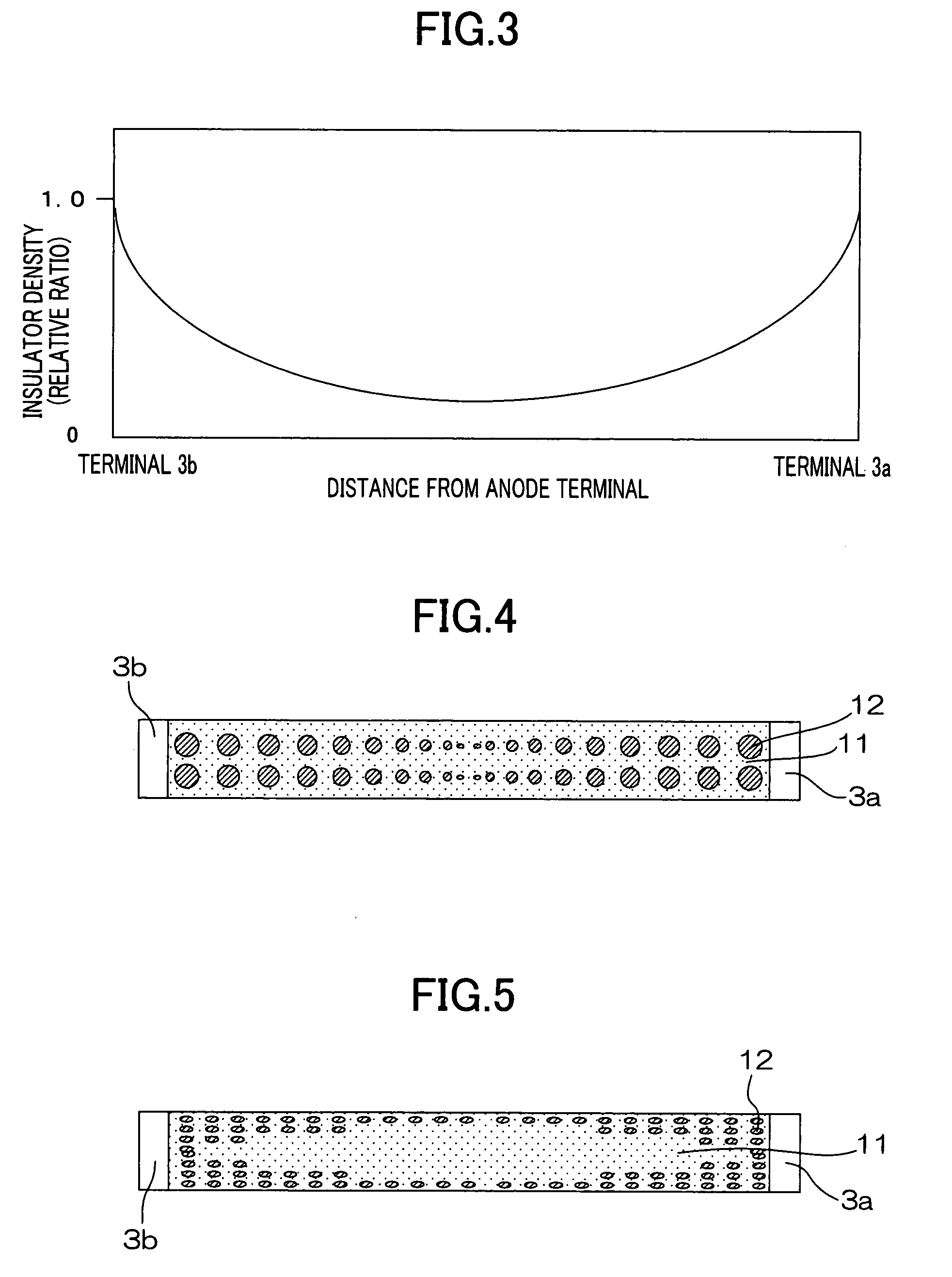
[0037]A first embodiment of the invention is a functional device comprising, on a substrate, a pair of electrodes, a functional layer which is sandwiched between the electrodes and has an output that varies in accordance with an applied electric current, and a terminal arranged to apply an electric current to at least one of the electrodes, in which an insulator is arranged between the electrodes and the density of the insulator becomes gradually decreases as the distance from the terminal increases. Preferably, the insulator forms a discontinuous phase between the electrodes. More preferably, the insulator is present as a layer comprising an electroconductive material which forms a continuous phase and the insulator which forms a discontinuous phase.

[0038]In the device according to the first embodiment of the invention, the distribution density of the insulator decreases as the distance from the terminal increases; therefore, this structure compensates for a voltage drop, so that a...

second embodiment

[0156]The functional device according to the second embodiment of the invention is a functional device comprising, on a substrate, a pair of electrodes, a functional layer which is sandwiched between the electrodes and has an output that varies in accordance with an applied electric current, and a terminal arranged to apply an electric current to at least one of the electrodes, in which at least one of the electrodes has a notch section, and the ratio of the area of the notch section to the area of the electrode decreases as the distance from the terminal increases. The shape of the functional device is not particularly limited as long as the functional device is a functional device affected by a voltage drop between the electrodes and the functional layer. When the distance from the terminal, the electrode resistance, and the I-V characteristic of the functional device are known, a voltage drop caused due to the shape of the functional device can be estimated. Thus, the notch secti...

example 1

1. Production of an Organic Emitting Device According to the First Embodiment of the Invention

(Formation of a Stripe Electrode)

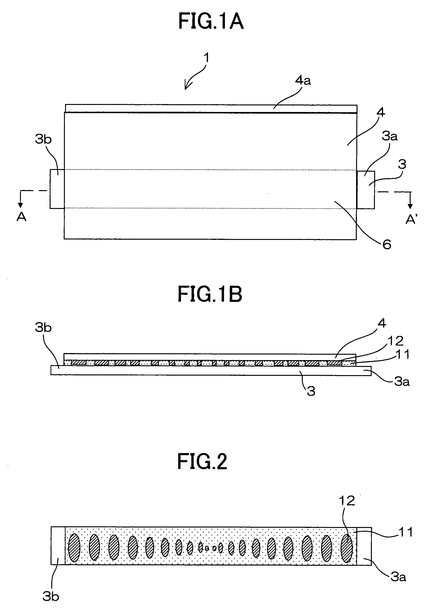
[0209]An anode made of ITO was formed into a film having a thickness of 200 nm on a non-alkaline substrate by sputtering, and then the resultant was subjected to wet etching, thereby making the film into the form of stripes each having a width of 100 μm and a length of 50 cm at intervals of 100 μm.

[0210]In the stripe electrode, both ends thereof having a length of 3.5 cm from edges thereof were each used as a terminal.

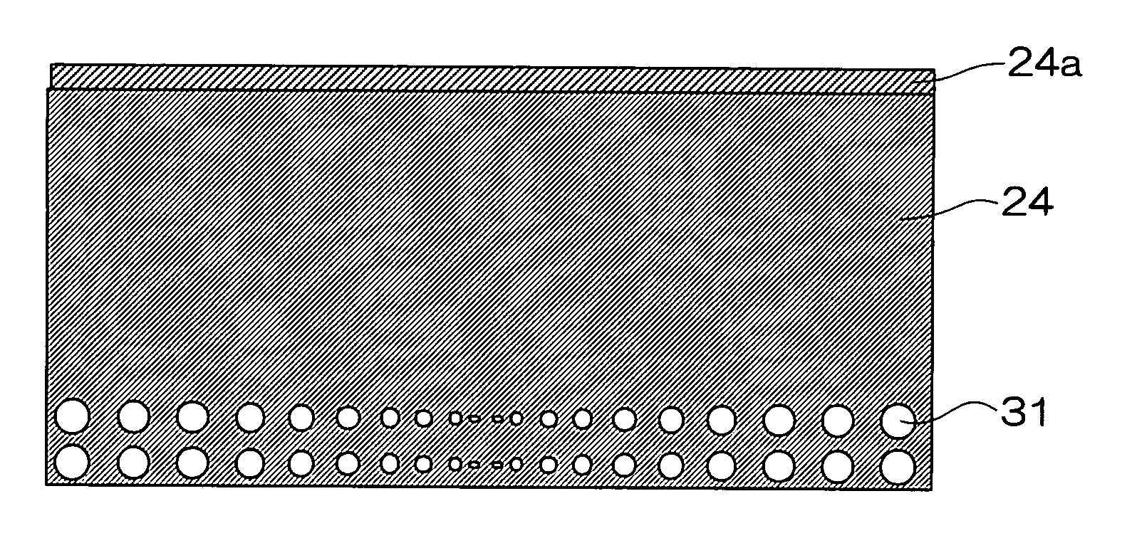
(Formation of an Insulating Layer)

[0211]A voltage drop was estimated from the above-mentioned shape, the distance from the anode terminal, the electrode resistance, and the I-V characteristic of a functional device to be formed. Corresponding to the resultant voltage drop distribution, an insulating layer was formed in such a manner that the density of the insulator was reduced as the voltage drop increased in the distribution. The insulating l...


PUM


Abstract

A functional device having, on a substrate, a pair of electrodes, a functional layer which is sandwiched between the electrodes and has an output that varies in accordance with an applied electric current, and a terminal arranged to apply an electric current to at least one of the electrodes, wherein an insulator is arranged between the electrodes and the density of the insulator decreases as the distance from the terminal increases, or wherein at least one of the electrodes has a notch section, and the ratio of the area of the notch section to the area of the electrode decreases as the distance from the terminal increases. This is an improved functional device which is excellent in production suitability and gives a uniform in-plane output, and can be rendered, in particular, an organic electroluminescence device.

Description

CROSS REFERENCE TO RELATED APPLICATIONS[0001]This application claims priority under 35 USC 119 from Japanese Patent Application Nos. 2006-100901 and 2006-100902, the disclosure of which is incorporated herein by reference.BACKGROUND OF THE INVENTION[0002]1. Field of the Invention[0003]The invention relates to a functional device, in particular, an organic electroluminescent device.[0004]2. Description of the Related Art[0005]In recent years, functional devices, in particular, organic electroluminescent devices have been developed.[0006]In organic electroluminescent devices, a thin film material which receives the supply of an electric current so as to be excited, thereby emitting light is used. Since the electroluminescent devices give high-luminance light at a low voltage, the devices have wide latent usages in broad fields which include the fields of cellar phone displays, personal digital assistants (PDAs), computer displays, automobile data displays, TV monitors, and ordinary il...

Claims


Application Information

Patent Timeline
Patent Type & Authority Applications(United States)
IPC IPC(8): H01L29/08
CPCH01L51/50H01L51/5096H01L2251/5361H01L51/5262H01L51/5203H10K50/18H10K50/00H10K50/805H10K50/85
Inventor TAKAHASHI, TOSHIROHAKAMATA, KAZUO
Owner UDC IRELAND
Why Eureka
Try Eureka