System and method for detecting single event latchup in integrated circuits

a single-event latchup and integrated circuit technology, applied in the direction of individual semiconductor device testing, instruments, electric discharge tubes, etc., can solve the problems of inability to detect the location of the sel in the circuit, the circuit in which the sel occurred may be destroyed by excessive current, and the cmos device becomes more susceptible to sels

Inactive Publication Date: 2007-10-04
INTEGRATED DEVICE TECH INC
View PDF15 Cites 7 Cited by
  • Summary
  • Abstract
  • Description
  • Claims
  • Application Information

AI Technical Summary

Benefits of technology

[0006] In another aspect, the present disclosure is directed to a system for testing an integrated circuit for potential latchup sites. In some embodiments, the system can include a radiation source adapted to generate and apply radiation to at least one area of the integrated circuit, a power supply adapted to apply a voltage to the int

Problems solved by technology

If an SEL occurs in the integrated circuit, excessive current may flow through the created low-impedance path, and the circuit in which the SEL has occurred may be destroyed by the excessive current.
While technology is trending toward the development of smaller and higher performance integrated circuits, CMOS devices become more susceptible to SELs.
The testing only can indicate whether an SEL occurred, but

Method used


Image

  • System and method for detecting single event latchup in integrated circuits
  • System and method for detecting single event latchup in integrated circuits
  • System and method for detecting single event latchup in integrated circuits

Examples


Embodiment Construction

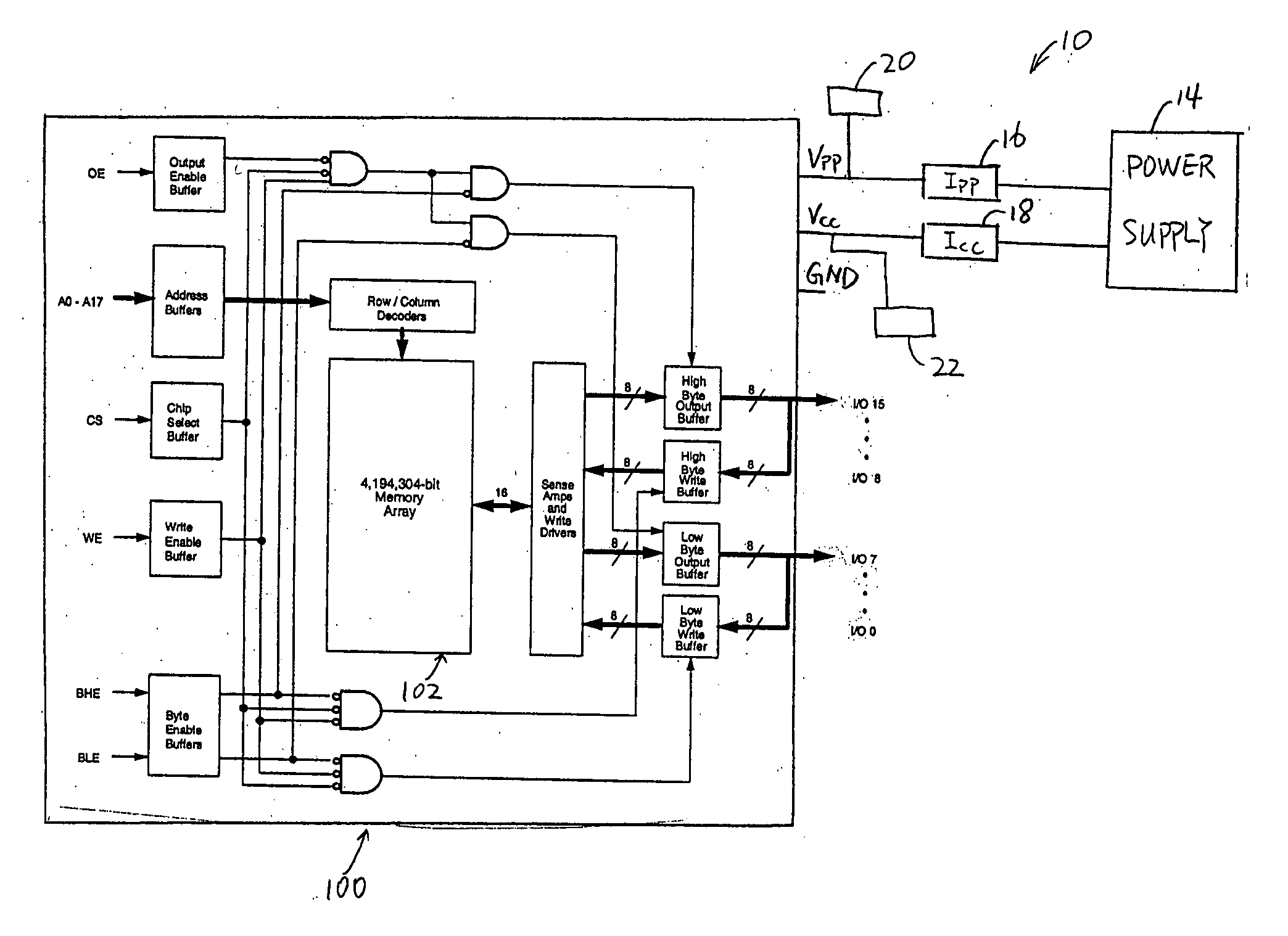
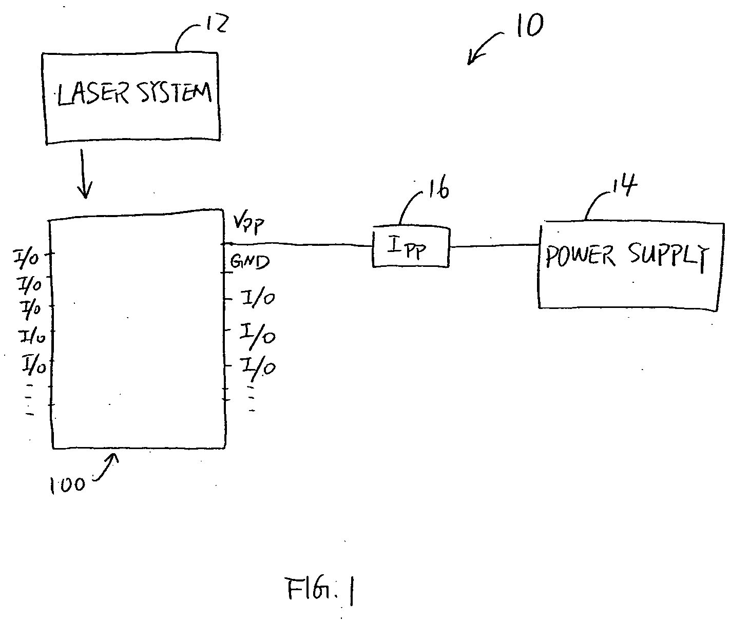
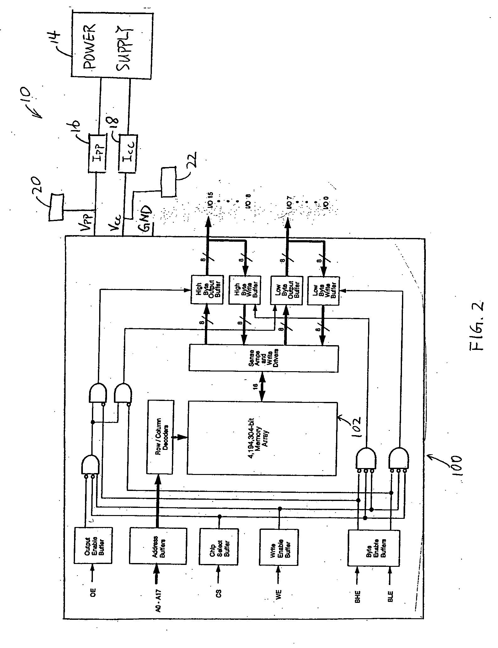
[0012] The present disclosure is directed to a system and method for testing an integrated circuit device for potential SEL sites. FIG. 1 shows a schematic diagram of an SEL testing system 10 according to some embodiments of the present invention for testing an integrated circuit 100. As shown in FIG. 1, system 10 includes a radiation source 12 adapted to apply one or more beams of radiation to at least one area of integrated circuit 100, a power supply 14 adapted to apply a voltage to integrated circuit 100, and a current measuring device 16 adapted to measure a current passing through integrated circuit 100.

[0013] In some embodiments, radiation source 12 can generate one or more laser beams, which can be used to scan at least one area of integrated circuit 100. In some embodiments, radiation source 12 produces beams of radiation that can be raster scanned over an area of integrated circuit 100. In some embodiments, radiation source 12 can generate pulsed laser beams (laser shots)...


PUM


Abstract

A method for testing an integrated circuit for potential latchup sites includes applying a voltage to the integrated circuit, measuring a current through the integrated circuit, applying at least one radiation beam to at least one area of the integrated circuit, and detecting an occurrence of a latchup by detecting an increase of the current through the integrated circuit upon applying the at least one radiation beam to the at least one area of the integrated circuit.

Description

FIELD OF THE INVENTION [0001] The present invention is related to detection of potential single event latchup (SEL) sites in integrated circuits and, in particular, to detecting and identifying single event latchup sites in integrated circuits using a radiation source. BACKGROUND OF THE INVENTION [0002] A latchup is an inadvertent creation of a low-impedance path in an integrated circuit as a result of triggering a parasitic device in the integrated circuit. Latchup may happen anywhere in the integrated circuit where a parasitic structure (which is a structure that is inadvertently formed by placement of two or more devices in close proximity, such as a parasitic PNPN structure, which forms a silicon-controlled rectifier (SCR)) exists. A single event latchup (SEL) may be caused by a number of triggering factors, such as cosmic rays, spikes of voltage on an input or output terminal of the integrated circuit, other event. If an SEL occurs in the integrated circuit, excessive current m...

Claims


Application Information

Patent Timeline
IPC IPC(8): G01R31/305
CPCG01R31/2881G01R31/308G01R31/305
Inventor CHU, TAN VANMUI, KEN-CHUEN
Owner INTEGRATED DEVICE TECH INC
Why Eureka
Try Eureka