Organic el display apparatus and driving method therefor

a display apparatus and organic el technology, applied in the direction of electric digital data processing, instruments, computing, etc., can solve the problems of image burn-in and prone to vary, and achieve the effect of accurate image display and less power

Inactive Publication Date: 2007-10-04
CANON KK
View PDF57 Cites 12 Cited by
  • Summary
  • Abstract
  • Description
  • Claims
  • Application Information

AI Technical Summary

Benefits of technology

[0018]The present invention provides a driving method for an organic EL display apparatus capable of accurate

Problems solved by technology

However, the relationship between the current and the potential of the gate varies according to the TFT, and sometimes changes with operating tim

Method used


Image

  • Organic el display apparatus and driving method therefor
  • Organic el display apparatus and driving method therefor
  • Organic el display apparatus and driving method therefor

Examples


first embodiment

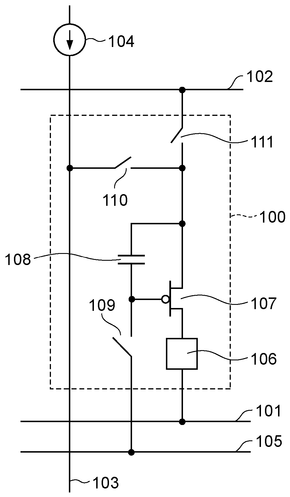
[0077]A circuit according to a first embodiment of the present invention which is based on the above-described concepts will be described. The same reference numerals are used for components having the same functions as those of FIG. 3.

[0078]An organic EL device and a driving circuit therefor in FIG. 1 include the following components: the organic EL device 106 having two terminals, an anode and a cathode; the driving transistor (TFT) 107 having three terminals, a gate, a source, and a drain; the voltage maintaining unit 108 configured with a capacitor disposed between the gate and the source of the driving transistor; one of the first constant voltage sources (V1) 101, one of the second constant voltage sources (V2) 102, and one of the third constant voltage sources (V3) 105, each of which maintains a fixed potential; one of the signal current sources 104 for providing a signal current; the first switch 109 disposed between the gate of the driving transistor 107 and one of the thir...

second embodiment

[0097]A circuit according to another embodiment of the present invention will be described with reference to FIG. 11. The same reference numbers are used for components having the same functions as those of FIG. 1.

[0098]In FIG. 11, at the time of light emission, the source of the driving TFT 107 is connected to the anode of the organic EL device 106 and the drain of the driving TFT 107 is connected to one of the second constant voltage sources 102. The driving TFT 107 is an n-channel TFT, but may be a p-channel TFT. If a p-channel TFT is used, voltage settings of the first and second constant voltage sources are interchanged, and the terminals of the organic EL device 106 are also interchanged.

[0099]The circuit shown in FIG. 11 operates in accordance with sequences shown in FIG. 12. In FIG. 12, the same reference numerals are used for items having the same descriptions as those of FIG. 5. Each of the first to third switches performs the same operations as those described with refere...

first example

[0122]FIG. 13 shows an example of a circuit according to an embodiment of the present invention which is configured with a low-temperature polysilicon CMOS. In the case of a display apparatus in which a driving circuit is formed on a substrate, and the organic EL device 106 is formed on the driving circuit, the display apparatus can be easily produced by connecting the drain of the driving TFT 107 to the anode of the organic EL device 106 as a pixel electrode and forming a metallic or transparent electroconductive film or the like on the entire top surface as the first constant voltage power sources 101. It is known that the organic EL device 106 included in the display apparatus created in the above-described order has excellent carrier injection characteristics. A voltage drop in the organic EL device is reduced, whereby the maximum output voltage of the signal current source and the power supply voltage can be further reduced.

[0123]A p-channel TFT is used for each of the driving ...


PUM


Abstract

An organic EL display apparatus has a driving circuit. In the driving circuit, the source and drain of a driving transistor and the anode and cathode of an organic EL device are connected in series between voltage sources. A current passes between the source and drain of the driving transistor and between the anode and cathode of the organic EL device in accordance with a voltage between the gate and source of the driving transistor. Consequently, the organic EL device emits light. In order to store the voltage in the capacitor, a constant voltage source is connected to the gate of the driving transistor and the above-described series connection is disconnected at the source of the driving transistor and connected to a signal source. Then, a current signal output from the signal source passes between the source and drain of the driving transistor, and charges are stored in a capacitor in accordance with the current signal.

Description

BACKGROUND OF THE INVENTION[0001]1. Field of the Invention[0002]The present invention relates to an organic EL (electroluminescence) display apparatus and a driving method therefor.[0003]2. Description of the Related Art[0004]An organic electroluminescence device utilizing electroluminescence (hereinafter abbreviated as EL) of an organic material has a first electrode, a second electrode, and an organic compound layer sandwiched between the electrodes. The organic compound layer includes a light emission layer and a carrier transport layer which are composed of organic molecules. The organic EL device is driven by a current passing between the electrodes. The luminance of the organic EL device is almost exactly proportional to the current (driving current). An organic EL display apparatus in which organic EL devices are arranged in a matrix form has excellent color reproducibility and excellent responsiveness to an input signal, and is therefore ideal particularly for display of mov...

Claims


Application Information

Patent Timeline
IPC IPC(8): G09G3/36
CPCG09G3/3233G09G2300/0819G09G2320/043G09G2310/0262G09G2300/0861
Inventor NAKAGAWA, KATSUMIKAWASAKI, SOMEIISEKI, MASAMIINABA, YUTAKA
Owner CANON KK
Why Eureka
Try Eureka