Semiconductor device fabricating method

Inactive Publication Date: 2007-10-04
TAIWAN SEMICON MFG CO LTD
View PDF1 Cites 46 Cited by
  • Summary
  • Abstract
  • Description
  • Claims
  • Application Information

AI Technical Summary

Benefits of technology

[0027]According to the semiconductor device fabricating method of the present invention, the polishing step, the laminating step, and the sealing step can be performed in a state where wafers where semiconductor chips are plurally formed or diced semiconductor chips are supported by a support substrate, so that the occurrence of warpage that had conventionally arisen in semiconductor chips due to the fabrication process is prevented, the essential planarity is maintained, further thinning of the wafers (semiconductor chips) is realized, and breakage of the wafers or semiconductor chips in the process can be effectively prevented.
[0028]Consequently, electrical connections can be made better. Further,

Problems solved by technology

According to conventionally known fabricating methods such as the semiconductor device fabricating method of JP-A No. 2004-296812, there is the potential for warpage to occur in the semiconductor chips or for the semiconductor chips themselves to break

Method used


Image

  • Semiconductor device fabricating method
  • Semiconductor device fabricating method
  • Semiconductor device fabricating method

Examples


Example

First Embodiment

(Configuration of Semiconductor Device)

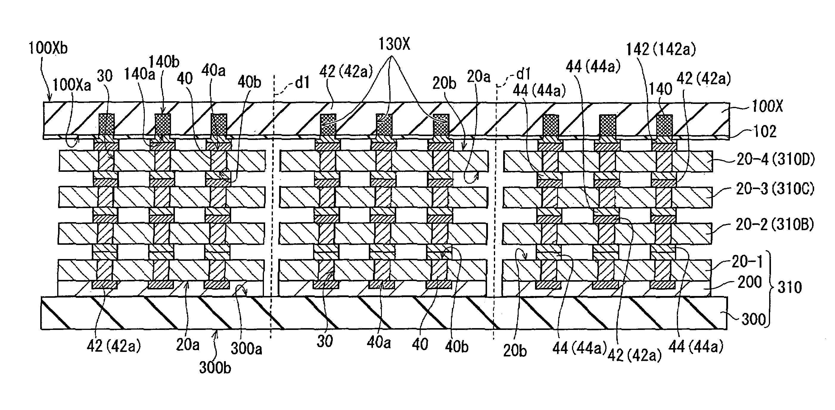
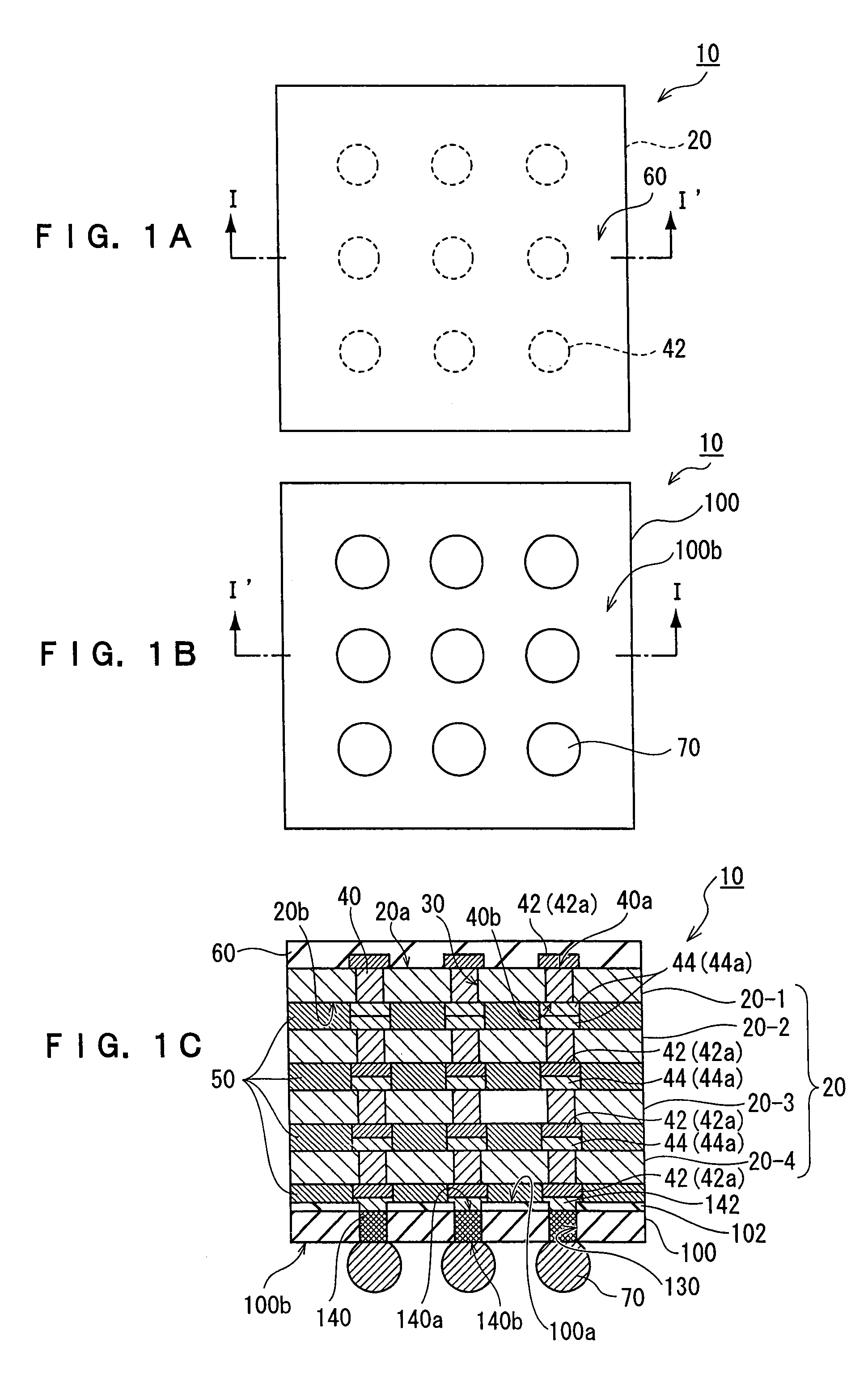
[0083]First, an example of the configuration of a semiconductor device fabricated by a semiconductor device fabricating method of a first embodiment of the present invention will be described with reference to FIG. 1A to FIG. 1C.

[0084]FIG. 1A is a schematic plan diagram showing a semiconductor device 10 as seen from the top surface side. FIG. 1B is a schematic plan diagram showing the semiconductor device 10 as seen from the bottom surface side. FIG. 1C is a schematic diagram showing a cross section cut by a one-dotted broken line represented by I-I′ in FIG. 1A and FIG. 1B.

[0085]The semiconductor device 10 includes a mounting substrate 100. The mounting substrate 100 is an interposer, for example. The mounting substrate 100 is shaped like a rectangular parallelepiped overall and includes a front surface 100a and a back surface 100b that opposes the front surface 100a.

[0086]An insulating film 102 comprising a silicon oxide film,...

Example

Second Embodiment

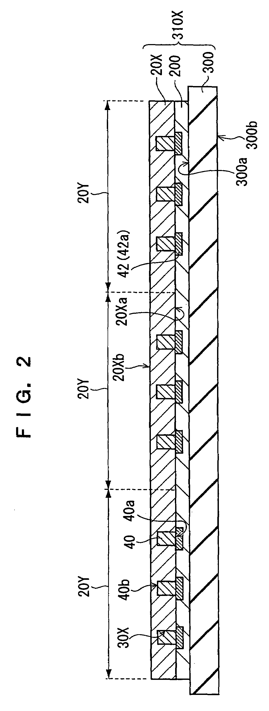
[0163]Another example of the method of fabricating the semiconductor device of the present invention having the above-described configuration will be described with reference to FIG. 11 to FIG. 14. It will be noted that, similar to FIG. 1C, each of these drawings is a schematic diagram showing a cross section cut at a position bisecting embedded electrodes.

[0164]The configuration of the semiconductor device to be fabricated is not different from the example configuration previously described in the first embodiment, so description thereof will be omitted.

[0165]FIG. 11 and FIG. 12 are schematic diagrams showing the cross section of a structure during fabrication.

[0166]FIG. 13 and FIG. 14 are schematic diagrams showing the cross section of the structure during fabrication continued from FIG. 12.

[0167]As shown particularly in FIG. 12, the semiconductor device fabricating method of this example is characterized in that it uses the precursor support substrate laminate 31...


PUM


Abstract

To improve the fabrication yield of semiconductor devices. A semiconductor device where a desired number of semiconductor chips are laminated in the thickness direction thereof is fabricated by repeating, an arbitrary number of times such as one time or two or more times, a step of bonding and mounting another support substrate laminate on first bumps exposed by separating and removing one support substrate from a support substrate laminate composite where second bumps of two support substrate laminates including plural semiconductor wafers mounted on support substrates have been made to face each other and are electrically connected.

Description

CROSS-REFERENCE TO RELATED APPLICATION[0001]This application claims priority under 35 USC 119 from Japanese Patent Application No. 2006-098384, the disclosure of which is incorporated by reference herein.BACKGROUND OF THE INVENTION[0002]1. Field of the Invention[0003]The present invention relates to a semiconductor device fabricating method, and in particular to a semiconductor device fabricating method where semiconductor chips having a plurally lamentable configuration are plurally laminated.[0004]2. Description of the Related Art[0005]A semiconductor chip laminate package is known where plural semiconductor chips are laminated with the purpose of multifunctionalizing a semiconductor device.[0006]As one example of such a semiconductor chip laminate package, there is a stacked multichip package. A stacked multichip package has a configuration where plural semiconductor chips are superposed and mounted on a substrate.[0007]Among methods of fabricating such a multichip package, a sem...

Claims


Application Information

Patent Timeline
IPC IPC(8): H01L21/784
CPCH01L21/76898H01L2924/01033H01L23/3135H01L24/97H01L25/0657H01L25/50H01L2224/16H01L2224/97H01L2225/06513H01L2225/06541H01L2225/06586H01L2924/01013H01L2924/01015H01L2924/01029H01L2924/01047H01L2924/01074H01L2924/01079H01L2924/01082H01L2924/15311H01L23/3128H01L2924/01019H01L2924/01006H01L2924/01005H01L2224/81H01L2224/05573H01L2224/05624H01L2224/05639H01L2224/05644H01L2224/05647H01L2224/05684H01L2224/06131H01L2224/13025H01L2224/81005H01L2924/181H01L2924/00H01L2924/00014
Inventor EGAWA, YOSHIMI
Owner TAIWAN SEMICON MFG CO LTD
Why Eureka
Try Eureka