Method to control source/drain stressor profiles for stress engineering

a technology of stress engineering and source/drain stressor, which is applied in the direction of semiconductor devices, electrical equipment, basic electric elements, etc., can solve the problems of extremely difficult integration of embedded sige (esige) into the normal cmos process flow, and achieve the effect of reducing repetition

Active Publication Date: 2007-10-11
IBM CORP +2
View PDF43 Cites 196 Cited by
  • Summary
  • Abstract
  • Description
  • Claims
  • Application Information

AI Technical Summary

Benefits of technology

[0038] The above and below advantages and features are of representative embodiments only, and are not exhaustive and/or exclusive. They are presented only to assist in understanding the invention. It should be understood that they are not representative of all the inventions defined by the claims, to be considered limitations on the invention as defined by the claims, or limitations on equivalents to the claims. For instance, some of these advantages may be mutually contradictory, in that they cannot be simultaneously present in a single embodiment. Similarly, some advanta...

Problems solved by technology

However, the integration of embedded SiGe (eSiGe) i...

Method used


Image

  • Method to control source/drain stressor profiles for stress engineering
  • Method to control source/drain stressor profiles for stress engineering
  • Method to control source/drain stressor profiles for stress engineering

Examples


Embodiment Construction
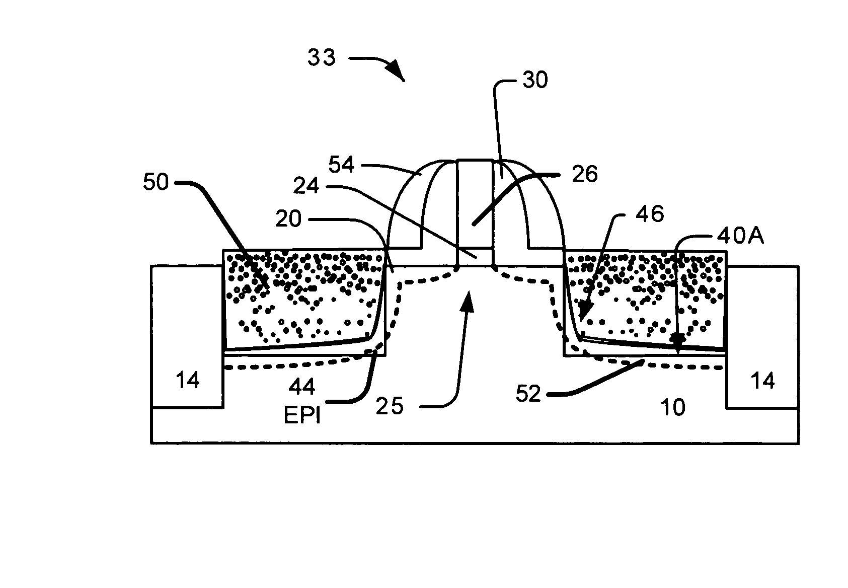
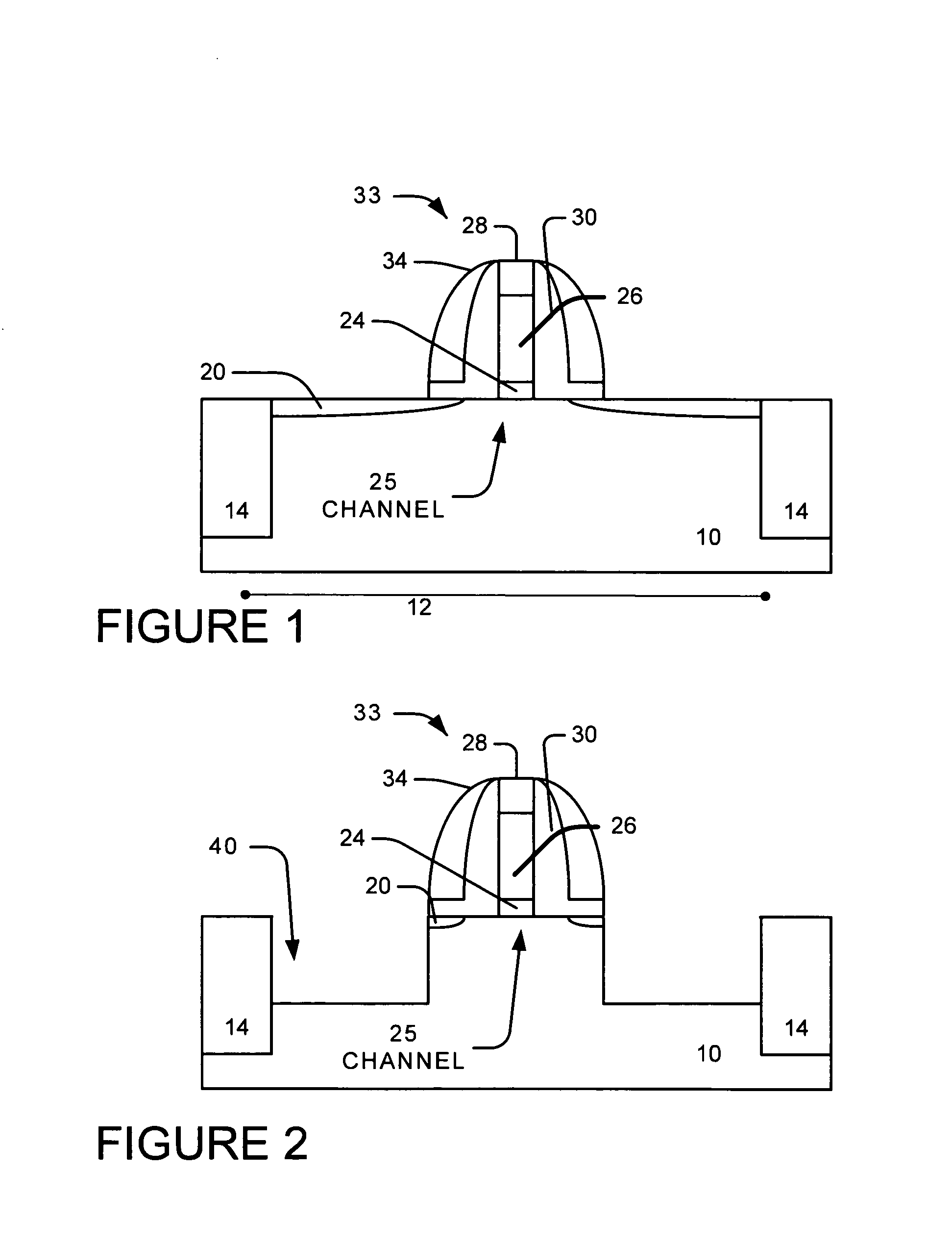
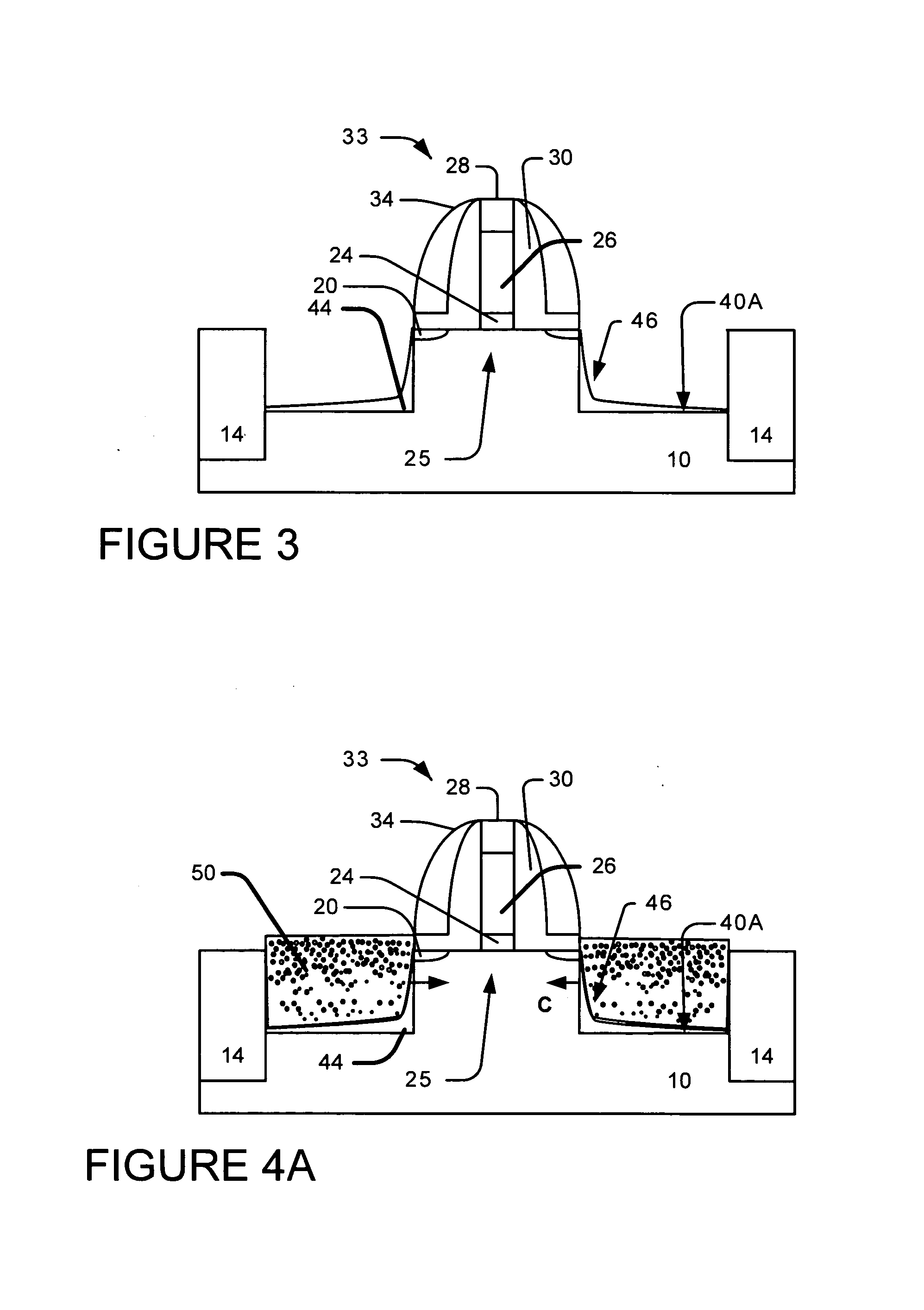
[0043] A. Overview

[0044] An example embodiment is a method to form a strained channel transistor using a stressor region. The recess for the stressor region is preferably formed using an anisotropic etch. An epitaxial layer is preferably formed in the recess. Then a graded stressor region is formed has a gradual change in dopant impurity concentration and / or in stress inducing atom concentration. The graded stressor region overlaps at least a portion of the source / drain region.

[0045] An example method embodiment comprises the following. [0046] form gate structure and Source / drain extension (SDE) regions [0047] form recess preferably using anisotropic etch [0048] form epitaxially grown layer in recess (lightly doped Si or SiGe buffer layer) [0049] form graded stressor layer in recess with graded dopant concentration and / or stressor atom concentration. [0050] reform spacers on gate structure [0051] the profile of the S / D stressor is not defined by the recess depth / profile [0052] ann...


PUM


Abstract

An example embodiment of a strained channel transistor structure comprises the following: a strained channel region comprising a first semiconductor material with a first natural lattice constant; a gate dielectric layer overlying the strained channel region; a gate electrode overlying the gate dielectric layer; and a source region and drain region oppositely adjacent to the strained channel region, one or both of the source region and drain region are comprised of a stressor region comprised of a second semiconductor material with a second natural lattice constant different from the first natural lattice constant; the stressor region has a graded concentration of a dopant impurity and/or of a stress inducing molecule. Another example embodiment is a process to form the graded impurity or stress inducing molecule stressor embedded S/D region, whereby the location/profile of the S/D stressor is not defined by the recess depth/profile.

Description

BACKGROUND OF INVENTION [0001] 1) Field of the Invention [0002] This invention generally relates to the devices and methods for the fabrication of semiconductor devices, and more particularly to the fabrication of Field Effect Transistors (FETs) having embedded Source / Drain regions with controlled impurity profiles. [0003] 2) Description of the Prior Art [0004] It is now well-known that SiGe can be embedded into the source / drain (S / D) regions of PFETs to generate uniaxial stress in the silicon channel. This in turn increases the carrier mobility in the PFET channel and thus enhances the PFET device performance significantly. However, the integration of embedded SiGe (eSiGe) into the normal CMOS process flow is extremely challenging. The extent of performance enhancement also depends strongly on the stress generated by the SiGe itself, the active dopant concentration in the eSiGe and the proximity of the stressor to the channel region. [0005] The importance of overcoming the various ...

Claims


Application Information

Patent Timeline
IPC IPC(8): H01L21/8234
CPCH01L21/823807H01L21/823814H01L29/165H01L29/7848H01L29/66636H01L29/7834H01L29/66628
Inventor CHONG, YUNG FULUO, ZHIJIONGHOLT, JUDSON ROBERT
Owner IBM CORP
Why Eureka
Try Eureka