Fabrication methods of a ZnO thin film structure and a ZnO thin film transistor, and a ZnO thin film structure and a ZnO thin film transistor

a technology of zno thin film and thin film structure, which is applied in the direction of vacuum evaporation coating, natural mineral layered products, coatings, etc., can solve the problems of difficult to achieve the desired semiconductor characteristics of zno, the method may be relatively difficult, and the failure to achieve the effect of success

Active Publication Date: 2007-10-18
SAMSUNG ELECTRONICS CO LTD
View PDF3 Cites 170 Cited by
  • Summary
  • Abstract
  • Description
  • Claims
  • Application Information

AI Technical Summary

Problems solved by technology

However, such higher temperature growth limits the materials that may be used to form a substrate and thus may not be applied to a plastic substrate which may be susceptible to heat damage.
However, this me

Method used


Image

  • Fabrication methods of a ZnO thin film structure and a ZnO thin film transistor, and a ZnO thin film structure and a ZnO thin film transistor
  • Fabrication methods of a ZnO thin film structure and a ZnO thin film transistor, and a ZnO thin film structure and a ZnO thin film transistor
  • Fabrication methods of a ZnO thin film structure and a ZnO thin film transistor, and a ZnO thin film structure and a ZnO thin film transistor

Examples


Embodiment Construction

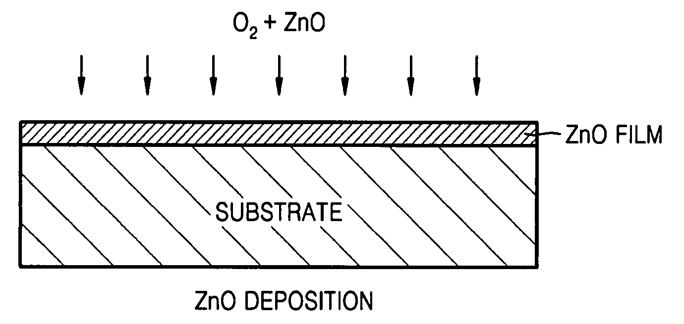
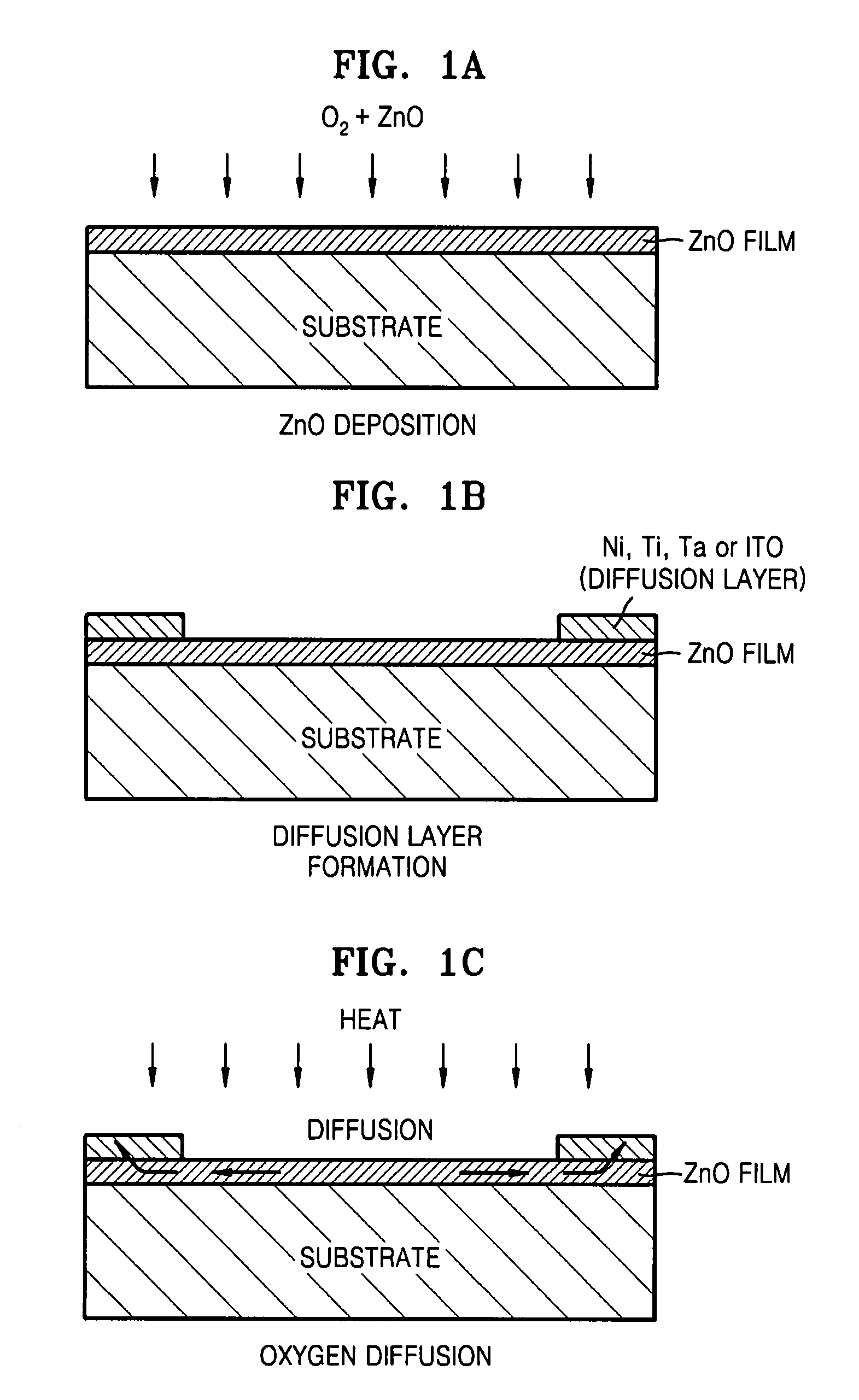
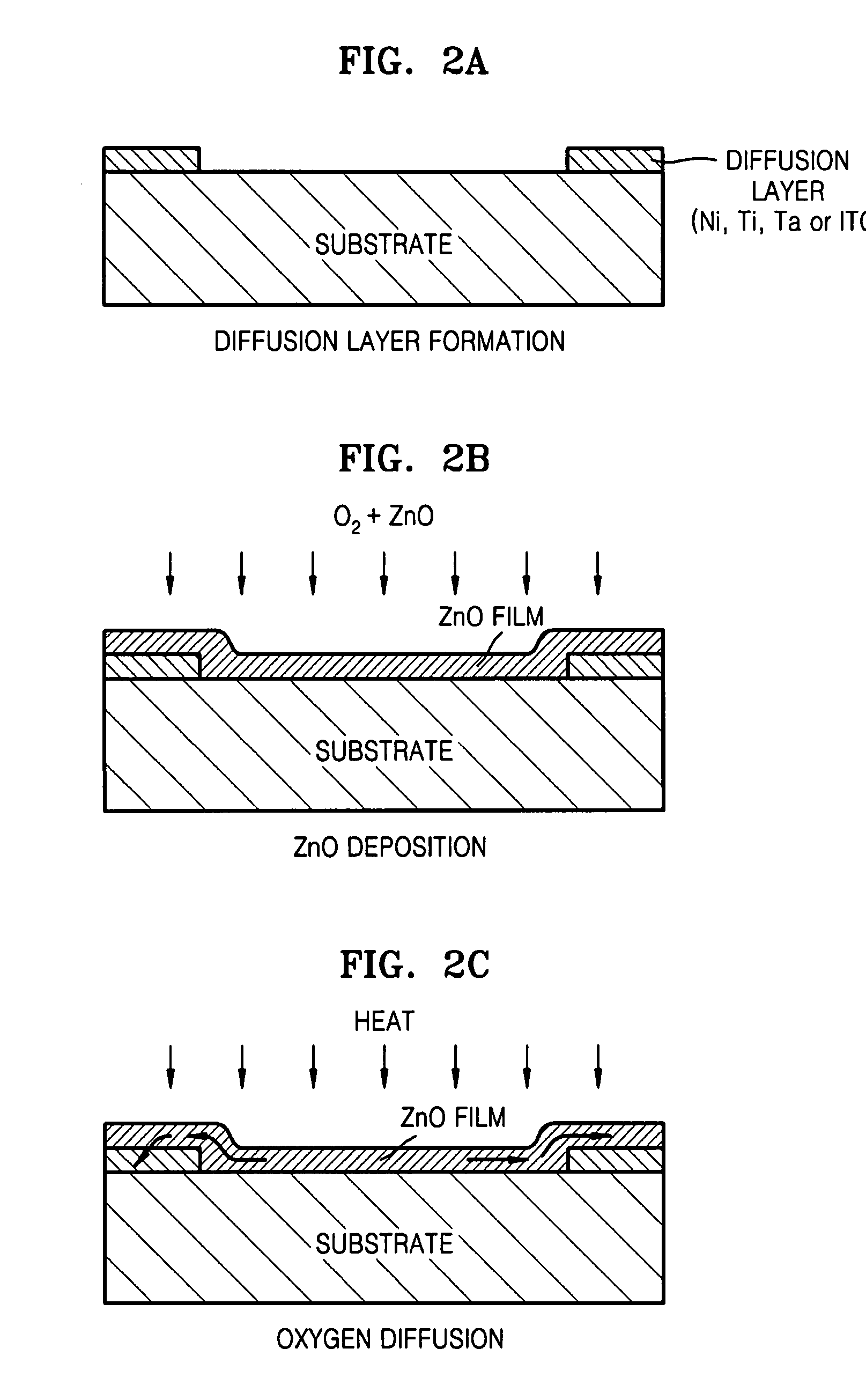
[0025]Hereinafter, methods of fabricating a ZnO thin film structure and a ZnO TFT, and a ZnO thin film structure and a ZnO TFT according to example embodiments will be described in detail with reference to the attached drawings. Example embodiments may, however, be embodied in many different forms and should not be construed as limited to the example embodiments set forth herein. Rather, these embodiments are provided so that this disclosure will be thorough and complete, and will fully convey the scope of example embodiments to those skilled in the art. In the drawings, the sizes and relative sizes of layers and regions may be exaggerated for clarity.

[0026]It will be understood that when an element or layer is referred to as being “on,”“connected to” or “coupled to” another element or layer, it can be directly on, connected or coupled to the other element or layer or intervening elements or layers may be present. In contrast, when an element is referred to as being “directly on,”“d...


PUM

PropertyMeasurementUnit
Densityaaaaaaaaaa
Electrical conductoraaaaaaaaaa
Affinityaaaaaaaaaa

Abstract

Provided is a method of fabricating a ZnO thin film structure and a ZnO thin film transistor (TFT), and a ZnO thin film structure and a ZnO thin film transistor. The method of fabricating a ZnO thin film structure may include forming a ZnO thin film on a substrate in an oxygen atmosphere, forming oxygen diffusion layers of a metal having an affinity for oxygen on the ZnO thin film and heating the ZnO thin film and the oxygen diffusion layers to diffuse oxygen of the ZnO thin film into the oxygen diffusion layers.

Description

PRIORITY STATEMENT[0001]This application claims priority under 35 USC § 119 to Korean Patent Application No. 10-2006-0035076, filed on Apr. 18, 2006, in the Korean Intellectual Property Office (KIPO), the entire contents of which are incorporated herein by reference.BACKGROUND[0002]1. Field[0003]Example embodiments relate to methods of fabricating a ZnO thin film structure and a ZnO thin film transistor (TFT), and a ZnO thin film structure and a ZnO TFT.[0004]2. Description of the Related Art[0005]Zinc oxide (ZnO) as a metal oxide semiconductor may be applied to TFTs, sensors, optical wave guides and / or piezoelectric elements. In general, a ZnO thin film grown at a higher temperature of about 400° C. or more may have higher quality. However, such higher temperature growth limits the materials that may be used to form a substrate and thus may not be applied to a plastic substrate which may be susceptible to heat damage.[0006]In the related art, a substrate may be heated at a temperat...

Claims


Application Information

Patent Timeline
IPC IPC(8): H01L29/10
CPCH01L29/45H01L29/78618H01L29/7869H01L21/02631H01L21/02422H01L21/02554H01L21/02381
Inventor KIM, CHANG-JUNGSONG, I-HUNKANG, DONG-HUNPARK, YOUNG-SOOLEE, EUN-HA
Owner SAMSUNG ELECTRONICS CO LTD
Why Eureka
Try Eureka