Magnetic memory device and method for fabricating the same

a memory device and magnetic technology, applied in the direction of galvano-magnetic devices, magnetic field-controlled resistors, semiconductor devices, etc., can solve the problems of increased write current, increased electric power consumption, increased power consumption,

Inactive Publication Date: 2007-10-18
FUJITSU LTD
View PDF5 Cites 50 Cited by
  • Summary
  • Abstract
  • Description
  • Claims
  • Application Information

AI Technical Summary

Problems solved by technology

However, in this method, the electric power consumption and reliability depend on the generation efficiency of the synthetic magnetic field generated by the bit line and the write word line and the ease of inversion of the free magnetization layer to the external magnetic field.
That is, as the integration is higher, the write current is increased, and the electric power consumption is increased.
However, the magnetization reversal magnetic field of the free magnetization layer is increased in inverse proportion with the decrease of the size, and the conventional current magnetic writing method drastically increases the write current, which will really mak

Method used


Image

  • Magnetic memory device and method for fabricating the same
  • Magnetic memory device and method for fabricating the same
  • Magnetic memory device and method for fabricating the same

Examples


Embodiment Construction

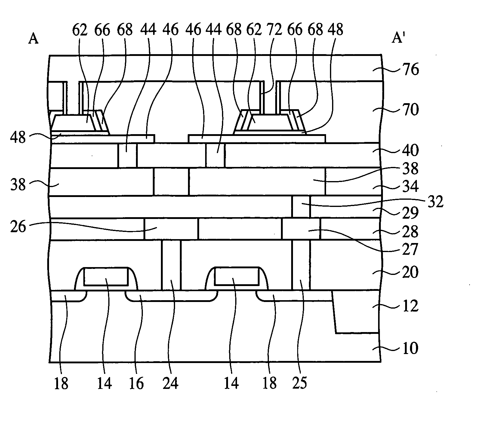
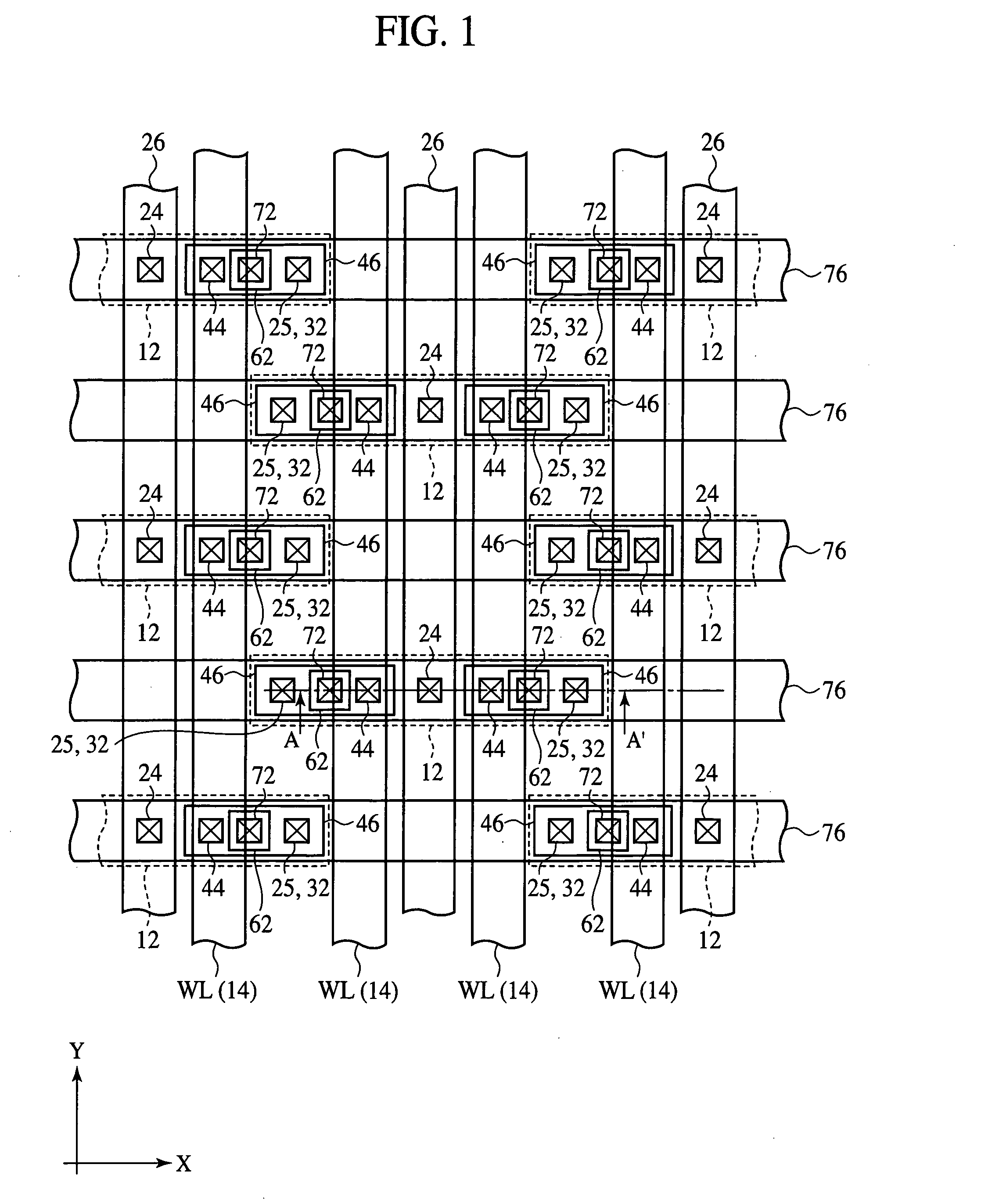
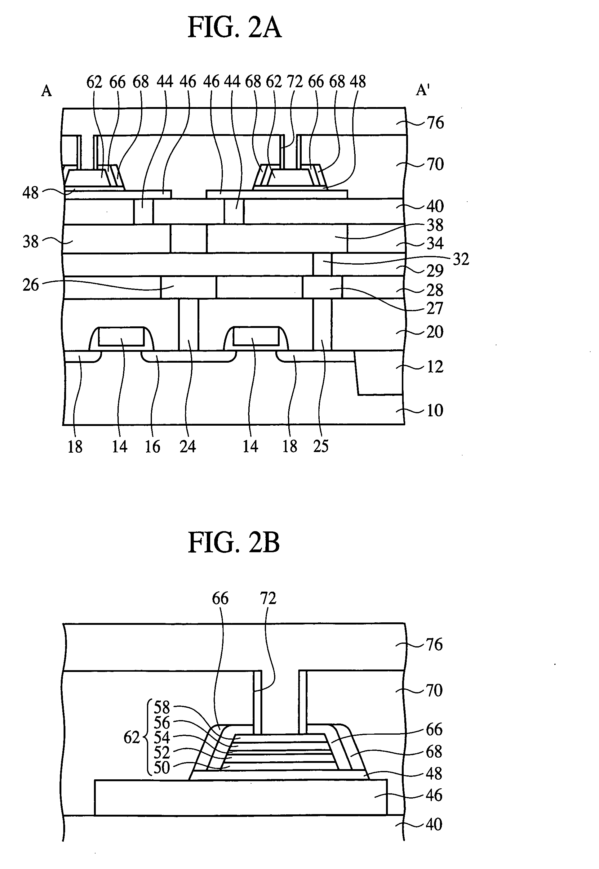
[0023]The magnetic memory device and the method for fabricating the same according to one embodiment of the present invention will be explained with reference to FIGS. 1 to 8C.

[0024]FIG. 1 is a plan view of the magnetic memory device according to the present embodiment, which shows a structure thereof. FIGS. 2A and 2B are diagrammatic sectional views of the magnetic memory device according to the present embodiment, which show the structure thereof. FIGS. 3A-3C, 4A-4B, 5A-5B, 6A-6B, 7A-7D and 8A-8C are sectional views showing the method for fabricating the magnetic memory device according to the present embodiment.

[0025]First, the structure of the magnetic memory device according to the present embodiment will be explained with reference to FIGS. 1 to 2B. FIG. 2A is the sectional view along the line A-A′ in FIG. 1, and FIG. 2B is an enlarged sectional view of a portion where the magnetoresistive effect element is formed.

[0026]A device isolation film 12 for defining a plurality of de...


PUM


Abstract

The magnetic memory device includes a magnetic shield film 48, and a magnetoresistive effect element 62 formed over the magnetic shield film 48 and including a magnetic layer 52, a non-magnetic layer 54 and a magnetic layer 56, in which a magnetization direction of the first magnetic layer or the second magnetic layer is reversed by spin injection, and a second magnetic shield film 68 formed over the side wall of the magnetoresistive effect element 62. Thus, the arrival of the leakage magnetic field from the interconnection near the magnetoresistive effect element 62 can be effectively prevented.

Description

CROSS-REFERENCE TO RELATED APPLICATIONS[0001]This application is based upon and claims the benefit of priority from the prior Japanese Patent Application No. 2006-093404, filed on Mar. 30, 2006, the entire contents of which are incorporated herein by reference.BACKGROUND OF THE INVENTION[0002]The present invention relates to a magnetic memory device and a method for fabricating the same, more specifically, a magnetic memory device using a spin injection-type magnetoresistive effect element and a method for fabricating the magnetic memory device.[0003]Recently, as a rewritable nonvolatile memory a magnetic random access memory (hereinafter called an MRAM) including magnetoresistive effect elements arranged in a matrix is noted. The MRAM uses combinations of magnetization directions of two magnetic layers to memorize information and, to read the information, detects resistance changes (i.e., current changes or voltage changes) between the resistance with the magnetization directions o...

Claims


Application Information

Patent Timeline
IPC IPC(8): H01L29/76H01L43/00H01L29/00
CPCB82Y10/00H01L43/12H01L43/08H01L27/228H10B61/22H10N50/01H10N50/10
Inventor UMEHARA, SHINJIROASHIDA, HIROSHIOCHIAI, TAKAOSATO, MASASHIGEKOBAYASHI, KAZUO
Owner FUJITSU LTD
Why Eureka
Try Eureka