Conduction cooled package laser and packaging method for forming the same

Inactive Publication Date: 2012-04-05
ARIMA LASERS CORP
View PDF4 Cites 4 Cited by
  • Summary
  • Abstract
  • Description
  • Claims
  • Application Information

AI Technical Summary

Benefits of technology

[0010]Hence, an objective of the present invention is to provide a packaging method for forming a CCP laser, thereby reducing the high heat influence on the characteristics of the semiconductor laser during fabrication, and reducing the occurrence of the brittle rupture of the semiconductor laser.
[0020]In the embodiments of the present invention, the Al / Ni nano-laminated foil is arranged between the first heat spreader and the second heat spreader for preventing the semiconductor laser device from being affected by the heat generated in the fabrication process by using the characteristic of the Al / Ni nano-laminated foil. Thus, the characteristics of the semiconductor laser device can be prevented from being affected by heat and the fabrication process of the present invention is brief and can be performed easily.

Problems solved by technology

However, just like many devices which unavoidably generate by-product heat during operation, the semiconductor laser diode also generates a lot of heat during high power operation even with a high electro-optic conversion rate.
If not being removed from the semiconductor laser (diode) immediately and properly, the heat will accumulate therein and ultimately increase the junction temperature thereof and cause the failure of the semiconductor laser (diode).
However, since the thermal expansion coefficients of the semiconductor laser (diode) and the heat sink are different, stress or strain will be generated therebetween when the temperature of the CCP laser rises.
Such self-generated stress or strain changes the electronic and optical characteristics of the semiconductor laser (diode) and thus causes the failure of the semiconductor laser (diode) or inherently shortens the operation life the semiconductor laser (diode).
Moreover, if a semiconductor laser (bar) with a large area such as 1-cm wide and 0.1 cm long is bonded, the aforementioned stress can cause mechanical problems.
Since the soldering process usually requires a long period high temperature process for melting the metal (solder) material, and thus the stress will be unavoidable generated within the semiconductor laser (diode).
In addition, the brittle rupture of the semiconductor material may also occur due to the high temperature environment in the process.

Method used


Image

  • Conduction cooled package laser and packaging method for forming the same
  • Conduction cooled package laser and packaging method for forming the same
  • Conduction cooled package laser and packaging method for forming the same

Examples


Embodiment Construction

[0028]Reference will be made in detail to the present embodiments of the invention, examples of which are illustrated in the accompanying drawings. Wherever possible, the same reference numbers are used in the drawings and the description to refer to the same or like parts.

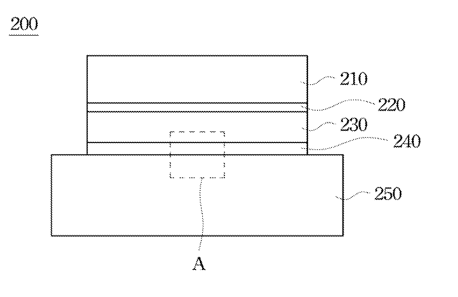
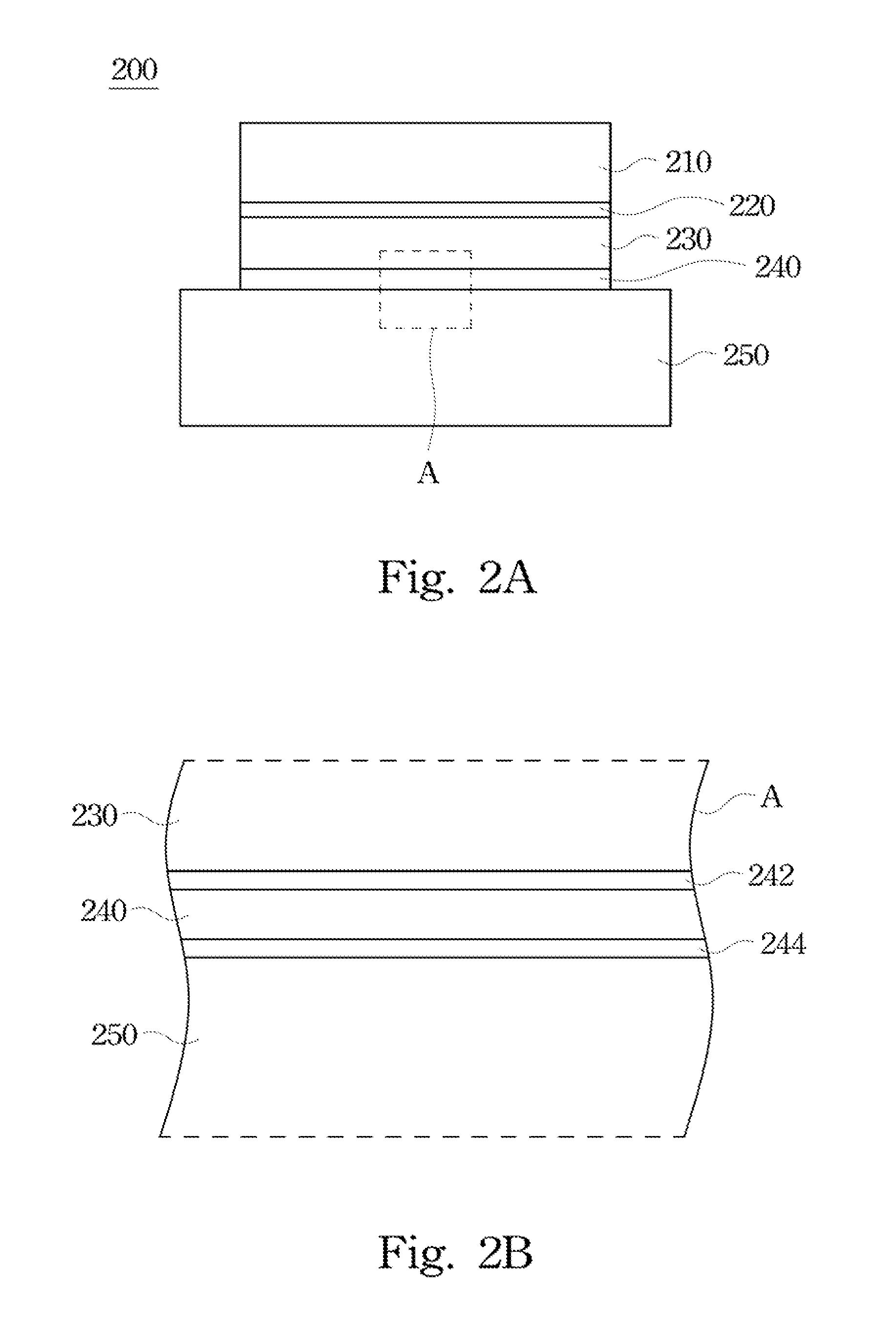
[0029]Embodiments of the present invention is featured in using the characteristics of an Al / Ni nano-laminated foil arranged in a CCP laser to prevent the laser output characteristic from being affected in the packaging process for forming the CCP laser.

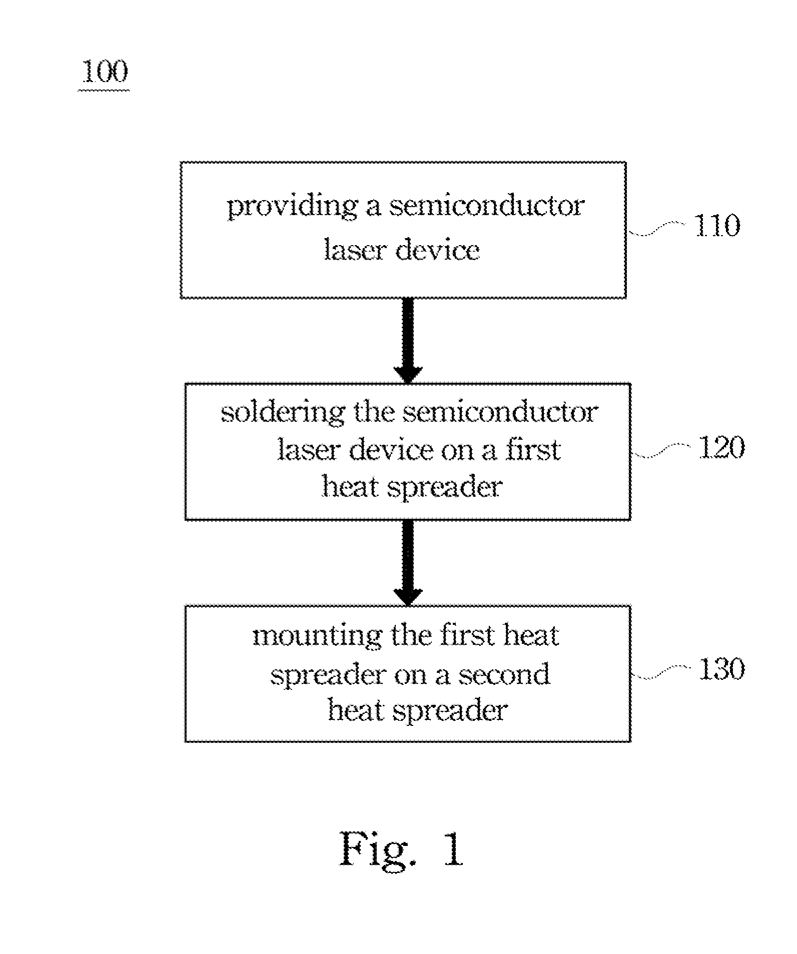
[0030]Referring to FIG. 1, FIG. 1 illustrates a process flow chart of a packaging method according to one embodiment of the present invention. At first, in step 110, a semiconductor laser device is provided. Then, in step 120, the semiconductor laser device is soldered on the first heat spreader. Thereafter, in step 130, the first heat spreader is bonded and fixed to the second heat spreader via an Al / Ni nano-laminated foil.

[0031]In step 120 an AuSn solder may be u...


PUM


Abstract

A packaging method for forming a conduction cooled package (CCP) laser is provided and includes soldering a semiconductor laser device on the first heat spreader; and then bonding the first heat spreader on the second spreader via an Al / Ni nano-laminated foil. Moreover, a CCP laser is also provided herein.

Description

RELATED APPLICATIONS[0001]This application claims priority to Taiwan Application Serial Number 99133315, filed Sep. 30, 2010, which is herein incorporated by reference.BACKGROUND[0002]1. Field of Invention[0003]The present invention relates to a laser device and a method for packaging the laser device. More particularly, the present invention relates to a conduction cooled package (CCP) laser and a packaging method for forming the same.[0004]2. Description of Related Art[0005]Since having a built-in resonant cavity, a semiconductor laser (diode) has the advantages of small size and high plug conversion efficiency. Moreover, with a solid-state gain medium, the semiconductor laser (diode) also has the advantage of long operation life. Thus, the semiconductor laser (diode) has been widely applied in various industries such as machine tooling, welding, scribing, printing, medicine, and recently, it also has been used in laser TV, laser cinema for high definition 3D display.[0006]However...

Claims


Application Information

Patent Timeline
IPC IPC(8): H01S3/04H01L33/48
CPCH01L23/36H01L2224/83801H01L2924/12042H01S5/02272H01S5/02476H01L2924/01079H01L2924/01322H01L2224/32245H01L24/29H01L24/32H01L24/83H01L2224/29144H01L2924/0105H01S5/0237
Inventor OU, SZUTSUN SIMONHSIAO, PO-WENHSIEH, CHIA-HUNGYANG, HUI-PINGHSU, YING-FENG
Owner ARIMA LASERS CORP
Why Eureka
Try Eureka