Method to monitor critical dimension of IC interconnect

Inactive Publication Date: 2007-10-25
CHARTERED SEMICONDUCTOR MANUFACTURING
View PDF9 Cites 1 Cited by
  • Summary
  • Abstract
  • Description
  • Claims
  • Application Information

AI Technical Summary

Benefits of technology

[0036] The above and below advantages and features are of representative embodiments only, and are not exhaustive and/or exclusive. They are presented only to assist in understanding the invention. It should be understood that they are not representative of all the inventions defined by the claims, to be considered limitations on the invention as defined by the claims, or limitations on equivalents to the claims. For instance, some of these advantages may be mutually contradictory, in that they cannot be simultaneously present in a single embodiment. Similarly, some advantages

Problems solved by technology

The main burden of this shrink roadmap is carried by the lithography, which is currently pushed to its physical limits.
The lithography process and exposure tools require an eve

Method used


Image

  • Method to monitor critical dimension of IC interconnect
  • Method to monitor critical dimension of IC interconnect
  • Method to monitor critical dimension of IC interconnect

Examples


example method

To Measure And Monitor Line Spacing On Samples

[0086] An example embodiment of is a method of monitoring the critical dimension (CD) of IC interconnects is describe below.

[0087] A. Steps

[0088] A flowchart of an example embodiment can comprise: (Also see FIG. 9)

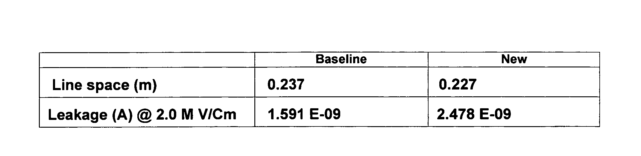
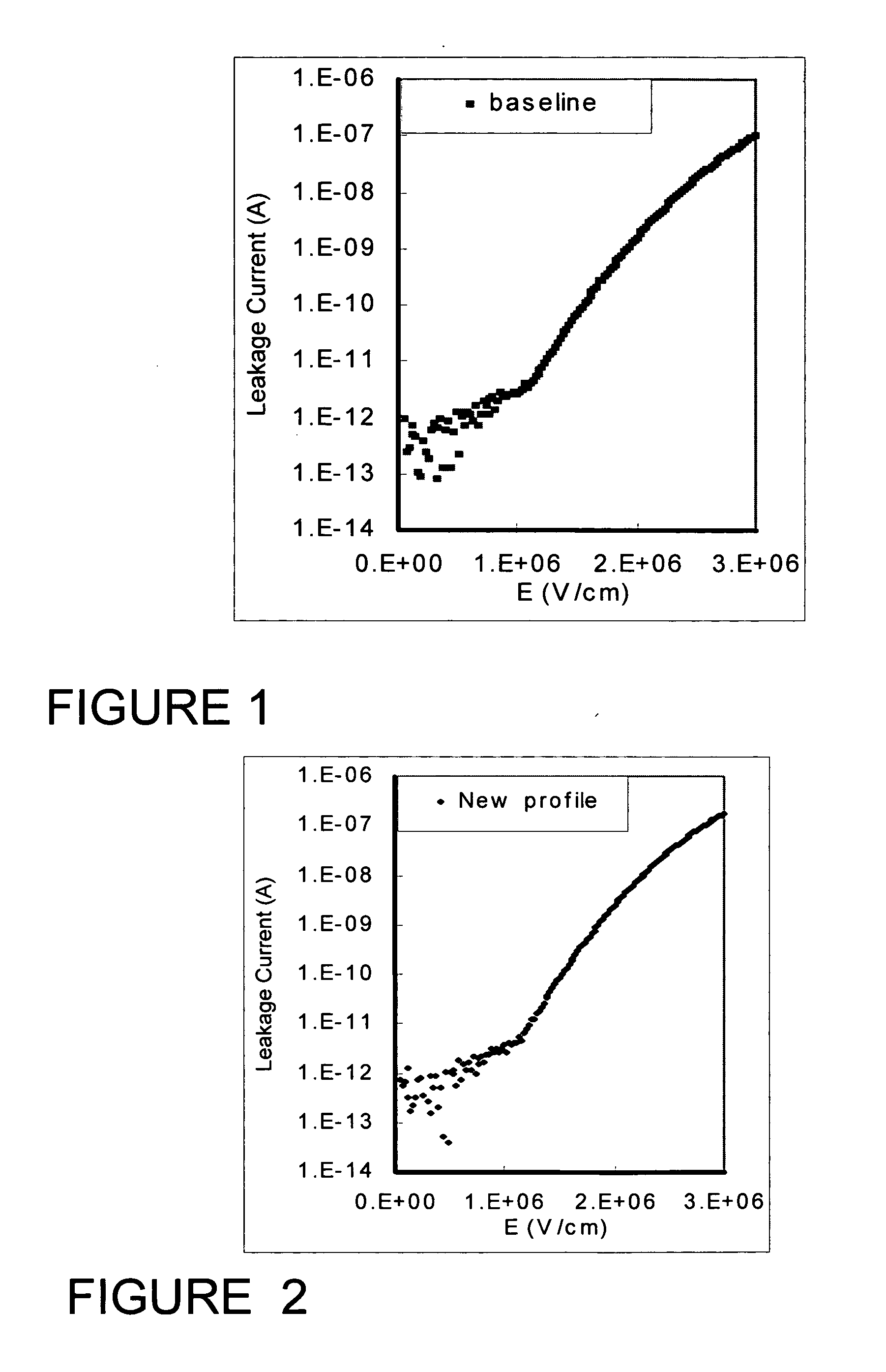
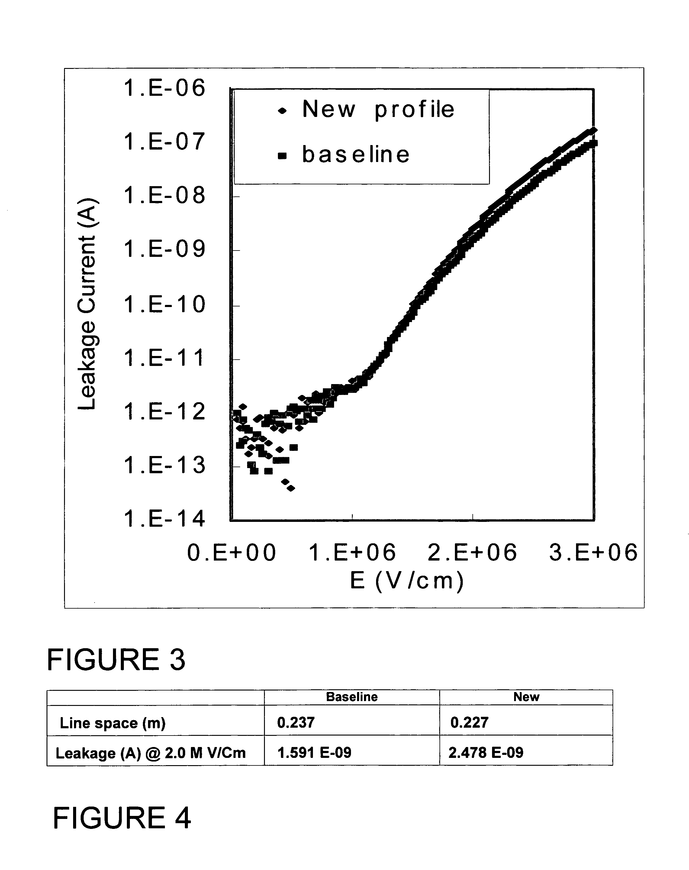
1) Test structure to measure I-V profile is specially designed

[0089] Comb structure is typical designed for I-V profile measurement

2) Establishment of I-V profile baseline in the specially designed structure [0090] Golden wafer is selected: [0091] Uniform CD [0092] No etch defect / CMP residue [0093] Good barrier layer [0094] I-V profile measurement [0095] Accurate CD measurement by SEM or TEM

3) I-V profile measurement of the structures in any locations / wafers

4) Compare the I-V profile with I-V profile baseline [0096] if profile is totally different from the baseline, process defect s exist [0097] If the profile is similar to baseline, Leakage currents are calculated from the I-V profiles at certain E

5) Line spacing ...


PUM


Abstract

An example method of monitoring and measuring the line width of interconnects comprising the following steps. First, we measure an I-V profile of a sample interconnect structure to obtain a sample I-V profile. The I-V profile is comprised of leakage current measurements at two or more voltages. The sample interconnect structure is comprised of spaced lines having a line spacing. Next we compare the sample I-V profile with a reference I-V profile at a reference line spacing to determine if sample interconnect structure is not defective. If the sample I-V profile is similar to the reference I-V profile, then leakage currents for the sample interconnect structure are derived from the I-V profiles at a selected voltages. Then we calculate the line spacing of the sample interconnect structure using the sample I-V profile.

Description

BACKGROUND OF INVENTION [0001] 1) Field of the Invention [0002] This invention relates generally to methods for the electrical measurement of critical dimensions and more particularly to electrical measurement of line spacing of conductive structures in semiconductor devices. [0003] 2) Description of the Prior Art [0004] An important driver for keeping Moore's Law is the improvement in productivity of semiconductor manufacturing. This is accomplished by the constant shrinking of device structures. The main burden of this shrink roadmap is carried by the lithography, which is currently pushed to its physical limits. The lithography process and exposure tools require an ever growing effort and support from metrology and inspection. New procedures are needed here to guarantee the required precision and accuracy specifications as well as the requirements for throughput and statistical significance. [0005] The low-voltage scanning electron microscope (SEM) is a main metrology tool for cr...

Claims


Application Information

Patent Timeline
IPC IPC(8): G01R31/02
CPCG01R31/2853
Inventor QIAN, HUACHUNG, CHING THIAM
Owner CHARTERED SEMICONDUCTOR MANUFACTURING
Why Eureka
Try Eureka