Composite heater and chill plate

a technology of temperature control and chill plate, which is applied in the direction of coating, metallic material coating process, chemical vapor deposition coating, etc., can solve the problems of reducing yield, reducing throughput, and inability to meet the stringent requirements of rapid uniform heating and cooling of wafers, so as to achieve high controllability, high controllability, and high controllability

Inactive Publication Date: 2007-11-01
SOKUDO CO LTD
View PDF9 Cites 345 Cited by
  • Summary
  • Abstract
  • Description
  • Claims
  • Application Information

AI Technical Summary

Benefits of technology

[0008] According to the present invention, methods and apparatus related to semiconductor manufacturing equipment are provided. More particularly, embodiments of the present invention relate to a method and apparatus for heating and / or cooling a substrate in a highly controllable manner. Embodiments of the invention contemplate multiple substrates being processed according to the same heating and cooling sequence in a highly controllable manner, thus helping to ensure a consistent wafer temperature for each substrate. While some embodiments of the invention are particularly useful in heating and / or cooling substrates in a chamber or station of a track lithography tool, other embodiments of the invention can be used in other applications where it is desirable to heat and cool substrates in a highly controllable manner.

Problems solved by technology

Although sophisticated heater and chiller assemblies are used to heat and cool wafers, they are unable to meet today's stringent requirements for rapid uniform heating and cooling of wafers.
The non-uniform heating and cooling of wafers causes either a reduction in throughput because the process must be delayed until temperature uniformity is achieved or a reduction in yields if the wafer is processed before the temperature across the entire wafer is substantially uniform.
One cause of the non-uniform heating and cooling is the limitation to how flat the wafer support can be made.
Another cause in the non-uniform cooling or heating of the wafer is the variation in the air gap from the heater or chill plate to the wafer.

Method used


Image

  • Composite heater and chill plate
  • Composite heater and chill plate
  • Composite heater and chill plate

Examples


Embodiment Construction

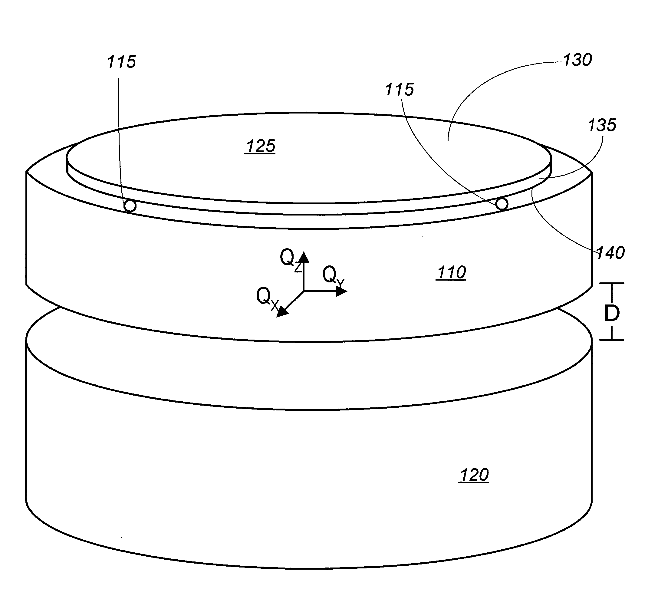
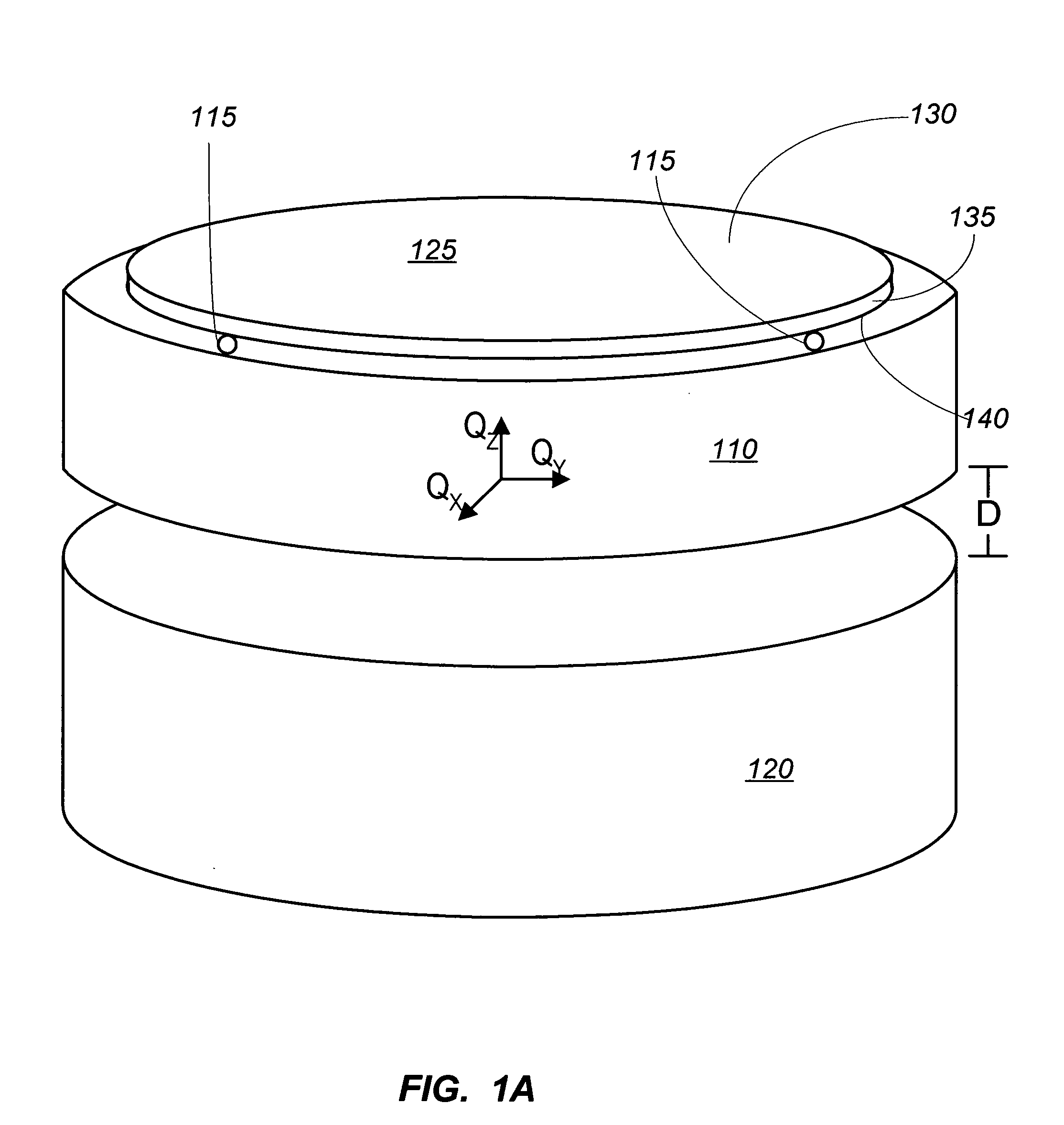
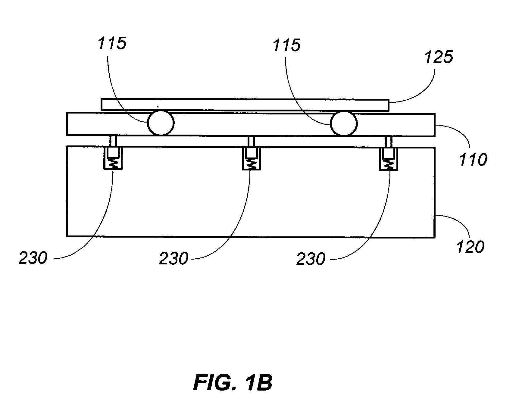
[0048] Controlling temperature uniformity across a wafer during semiconductor processing can be very useful in producing uniform properties of devices made on wafers. For example, when cooling or heating a wafer during a semiconductor manufacturing process, it can be advantages if the wafer is uniformly cooled or heated so that all portions of the wafer are processed at nearly the same temperature. The present invention provides a system and method for efficiently, rapidly and uniformly cooling or heating a wafer during semiconductor processing. Although the invention is described in terms of cooling or heating wafers in a track lithography tool, the invention can be implemented in tools which cool or heat a wafer during processing. Further details of the track lithography tool configuration can be found in copending U.S. patent application Ser. No. 11 / 174,681 filed on Jul. 5, 2005 which is hereby incorporated by reference in its entirety.

[0049]FIG. 1A is a block diagram illustrati...


PUM

PropertyMeasurementUnit
thicknessaaaaaaaaaa
thicknessaaaaaaaaaa
temperatureaaaaaaaaaa

Abstract

An integrated system for baking and chilling wafers includes a heater for heating a wafer to an elevated temperature, a chiller for cooling the wafer, and a shuttle operatively connected to the heater and the chiller for transferring the wafer between the heater and the chiller. The chiller further includes a low thermal mass wafer support for providing support to a bottom surface of a wafer and a chill plate coupled to the low thermal mass wafer support for cooling the wafer. The low thermal mass wafer support has a higher thermal conductivity in the plane parallel to the bottom surface of the wafer than in the direction perpendicular to the bottom surface of the wafer. The low thermal mass wafer support can further include a plurality of proximity pins for supporting the wafer.

Description

BACKGROUND OF THE INVENTION [0001] The present invention relates generally to the field of substrate processing equipment. More particularly, the present invention relates to a method and apparatus for controlling the temperature of substrates, such as semiconductor substrates, used in the formation of integrated circuits. [0002] Modern integrated circuits contain millions of individual elements that are formed by patterning the materials, such as silicon, metal and / or dielectric layers, that make up the integrated circuit to sizes that are small fractions of a micrometer. The technique used throughout the industry for forming such patterns is photolithography. A typical photolithography process sequence generally includes depositing one or more uniform photoresist (resist) layers on the surface of a substrate, drying and curing the deposited layers, patterning the substrate by exposing the photoresist layer to electromagnetic radiation that is suitable for modifying the exposed lay...

Claims


Application Information

Patent Timeline
Patent Type & Authority Applications(United States)
IPC IPC(8): C23C16/00
CPCH01L21/67109
Inventor HERCHEN, HARALDSOMAYAJI, SHARATHCHANDRAISHIKAWA, TETSUYALUE, BRIAN C.
Owner SOKUDO CO LTD
Why Eureka
Try Eureka