Read-preferred SRAM cell design

Active Publication Date: 2007-11-01
TAIWAN SEMICON MFG CO LTD
View PDF10 Cites 24 Cited by
  • Summary
  • Abstract
  • Description
  • Claims
  • Application Information

AI Technical Summary

Benefits of technology

[0010]The advantageous features of the present invention include an improved read m

Problems solved by technology

Reduced read and write margins may cause errors in respective read and write operations when the read and write operations are affected by static noise.
However

Method used


Image

  • Read-preferred SRAM cell design
  • Read-preferred SRAM cell design
  • Read-preferred SRAM cell design

Examples


Example

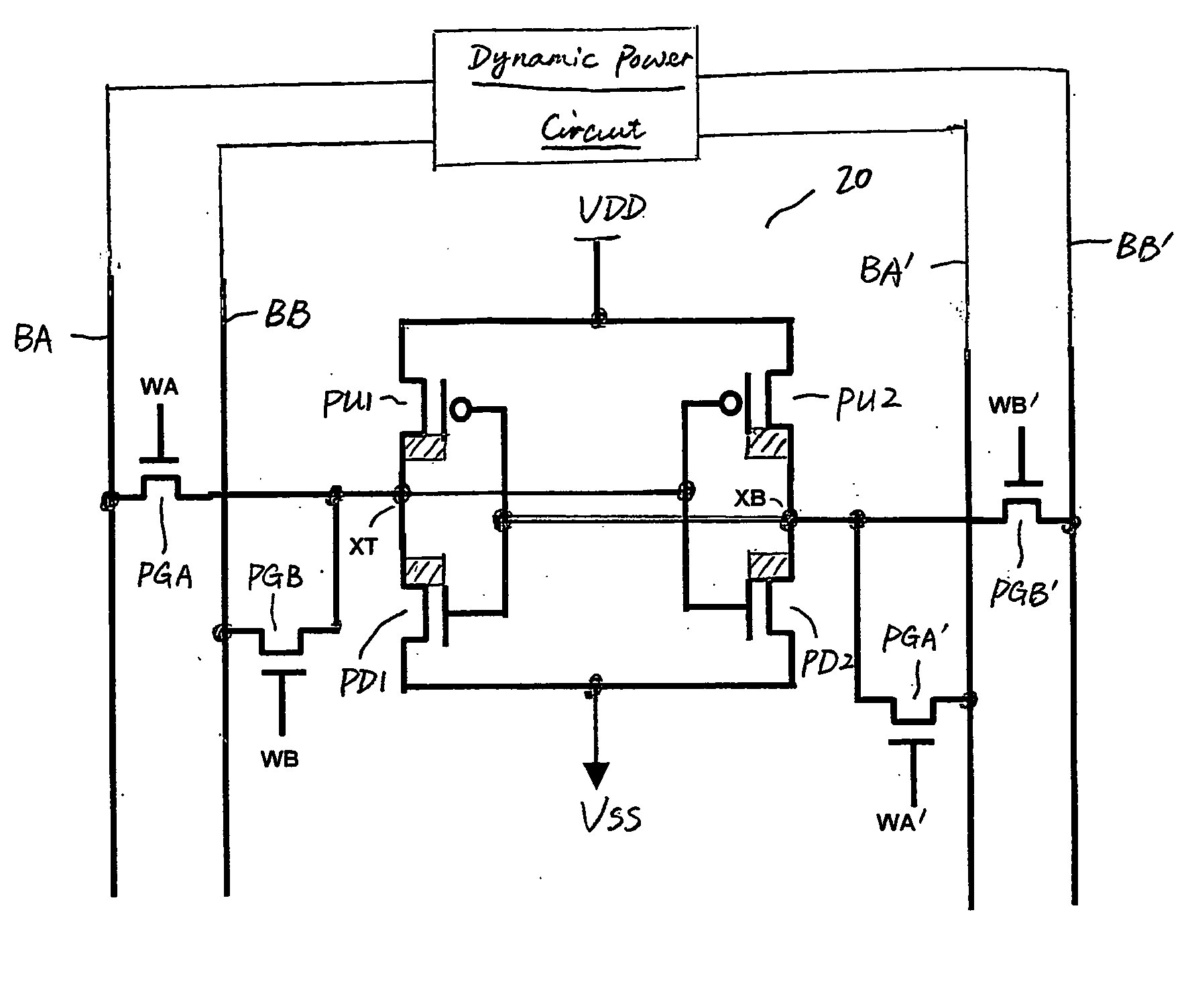
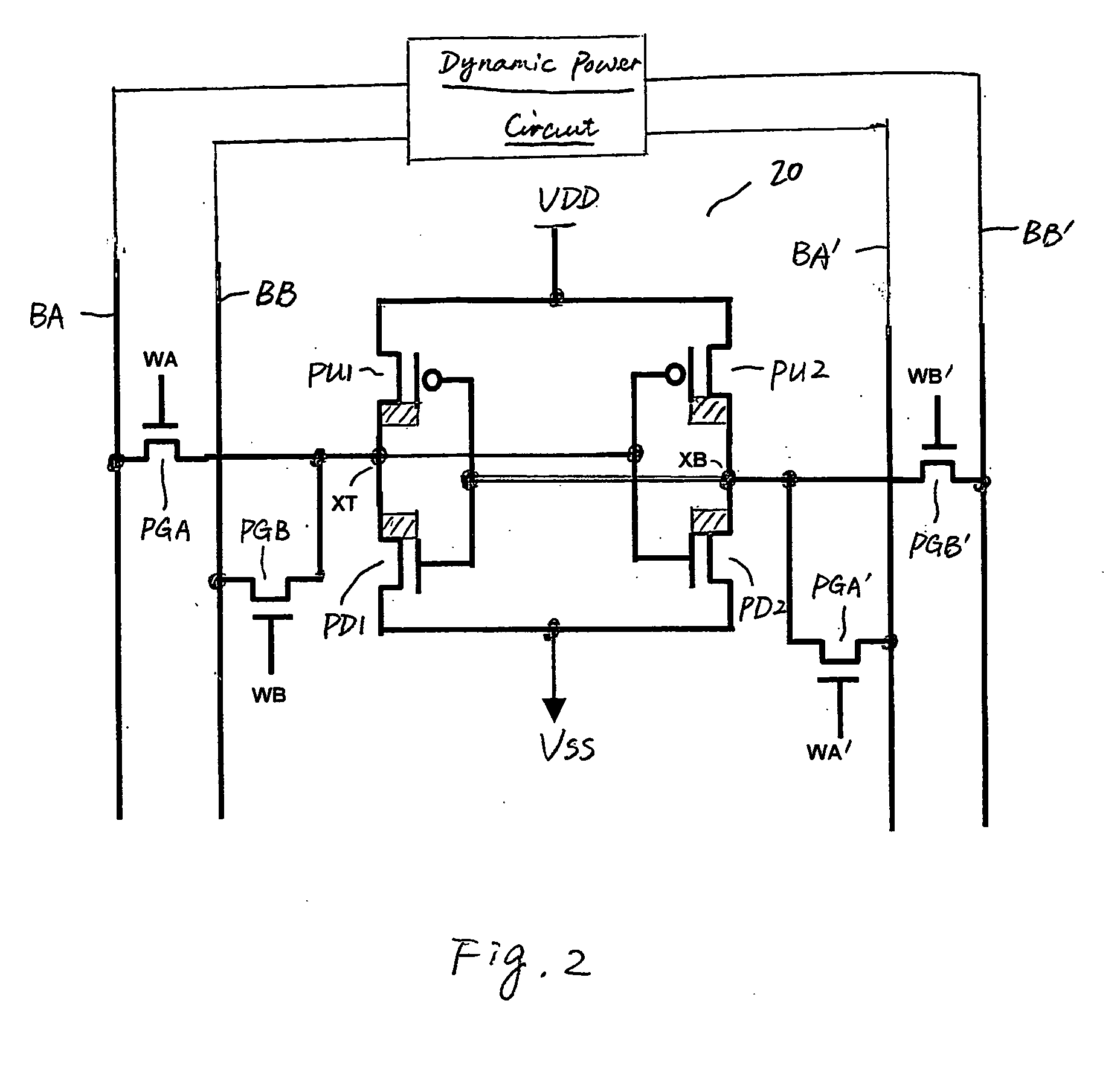
[0023]In a first embodiment, the increase in the α ratio and / or β ratio is achieved by increasing the physical width-to-length ratios (also referred to as W / L ratios) of the pull-down and / or pull-up MOS devices, respectively. In an exemplary embodiment, the W / L ratios of the pull-down MOS devices PD1 and PD2 and the W / L ratios of the pass-gate MOS devices PGA, PGB, PGA′, and / or PGB′ preferably have ratios of between about 1.8 and 5. In another exemplary embodiment formed using 90 nm technology, pull-down MOS devices PD1 and PD2 have a gate width of about 180 nm and a gate length of about 100 nm, while pass-gate MOS devices PGA, PGB, PGA′, and PGB′ have a gate width of about 120 nm and a gate length of about 115 nm. The resulting W / L ratios of the pull-down MOS devices PD1 and PD2 and the W / L ratios of the pass-gate MOS devices PGA, PGB, PGA′, and / or PGB′ have α ratio of 1.725.

Example

[0024]In a second embodiment, the increase in the α ratio and β ratio is achieved by weakening pass-gate MOS devices PGA, PGB, PGA′, and / or PGB′, and thus reducing their device drive currents. This may be achieved by reducing the W / L ratios of the respective pass-gate MOS devices. In addition, weakening the pass-gate MOS devices can be achieved either by skipping process steps commonly used for improving MOS devices, or adopting methods such as forming stressed ILD layer for pass-gate NMOS devices.

Example

[0025]In a third embodiment, the increase in the α ratio and / or β ratio is achieved by forming asymmetric pull-up MOS devices PU1, PU2 and / or pull-down MOS devices PD1 and PD2. Referring back to FIG. 2, shaded rectangles are marked adjacent the source regions of the pull-up and pull-down MOS devices, symbolizing that respective MOS devices are asymmetric MOS devices.

[0026]An exemplary embodiment of an asymmetric MOS device 30 is shown in FIG. 3. MOS device 30 includes a gate electrode 32 on a gate dielectric 33, gate spacers 35 on sidewalls of the gate electrode 32 and gate dielectric 33, lightly-doped source / drain (LDD) regions 34, and pocket regions 36, 38, 40 and 42 in substrate 44. The illustrated MOS device 30 has asymmetric structures on the source side and drain side. An exemplary formation process is described as follows.

[0027]First, semiconductor substrate 44 is provided. A gate structure including a gate electrode 32 and a gate dielectric 33 is formed on semiconductor subs...


PUM


Abstract

A read-preferred SRAM cell includes a pull-up MOS device having a first drive current, a pull-down MOS device coupled to the pull-up MOS device, the pull-down MOS device having a second drive current, and a pass-gate MOS device having a third drive current coupled to the pull-up MOS device and the pull-down MOS device. The first drive current and the third drive current preferably have an α ratio of between about 0.5 and about 1. The second drive current and the third drive current preferably have a β ratio of between about 1.45 and 5.

Description

[0001]This application claims the benefit of U.S. Provisional Application Ser. No. 60 / 795,835, filed on Apr. 28, 2006, entitled “Read-Preferred SRAM Cell Design,” which application is hereby incorporated herein by reference.TECHNICAL FIELD[0002]This invention relates generally to semiconductor devices, and more particularly to memory cells, and even more particularly to layout design and manufacturing methods of static random access memory cells.BACKGROUND[0003]Static random access memory (SRAM) is commonly used in integrated circuits. SRAM cells have the advantageous feature of holding data without a need for refreshing. FIG. 1 illustrates an exemplary circuit diagram of a typical six-MOS device SRAM cell, which includes pass-gate MOS devices 10 and 24, pull-up MOS devices 12 and 16, and pull-down MOS devices 14 and 18. Gates 2 and 4 of the respective pass-gate MOS devices 10 and 24 are controlled by a word-line WL that determines whether the current SRAM cell is selected. A latch ...

Claims


Application Information

Patent Timeline
IPC IPC(8): G11C11/00
CPCG11C11/412H01L29/66659H01L21/26586
Inventor WANG, PING-WEIMII, YUH-JIERLIAO, HUNG-JEN
Owner TAIWAN SEMICON MFG CO LTD
Why Eureka
Try Eureka