Stabilized photovoltaic device and methods for its manufacture

a photovoltaic device and stabilization technology, applied in the field of semiconductor devices, can solve the problems of reducing the performance of the photovoltaic device in which the semiconductor is incorporated, affecting the performance of the photovoltaic device, and not always being able to meet the needs of specific applications

Inactive Publication Date: 2007-11-08
UNITED SOLAR OVONIC
View PDF12 Cites 66 Cited by
  • Summary
  • Abstract
  • Description
  • Claims
  • Application Information

AI Technical Summary

Problems solved by technology

However, nanocrystalline materials have, heretofore, been poorly understood, and as a consequence, their potential has not always been realized in particular applications.
It has been found that in certain applications, nanocrystalline materials can exhibit light-induced metastabilities which degrade the performance of photovoltaic devices in which they are incorporated.
In other instances, overall performance of photovoltaic devices which include nanocrystalline materials have not met theoretical expectations.
In some instances, the semiconductor materials comprising the intrinsic layer can exhibit light-induced metastabilities which degrade the performance of the photovoltaic device.

Method used


Image

  • Stabilized photovoltaic device and methods for its manufacture
  • Stabilized photovoltaic device and methods for its manufacture
  • Stabilized photovoltaic device and methods for its manufacture

Examples


Embodiment Construction

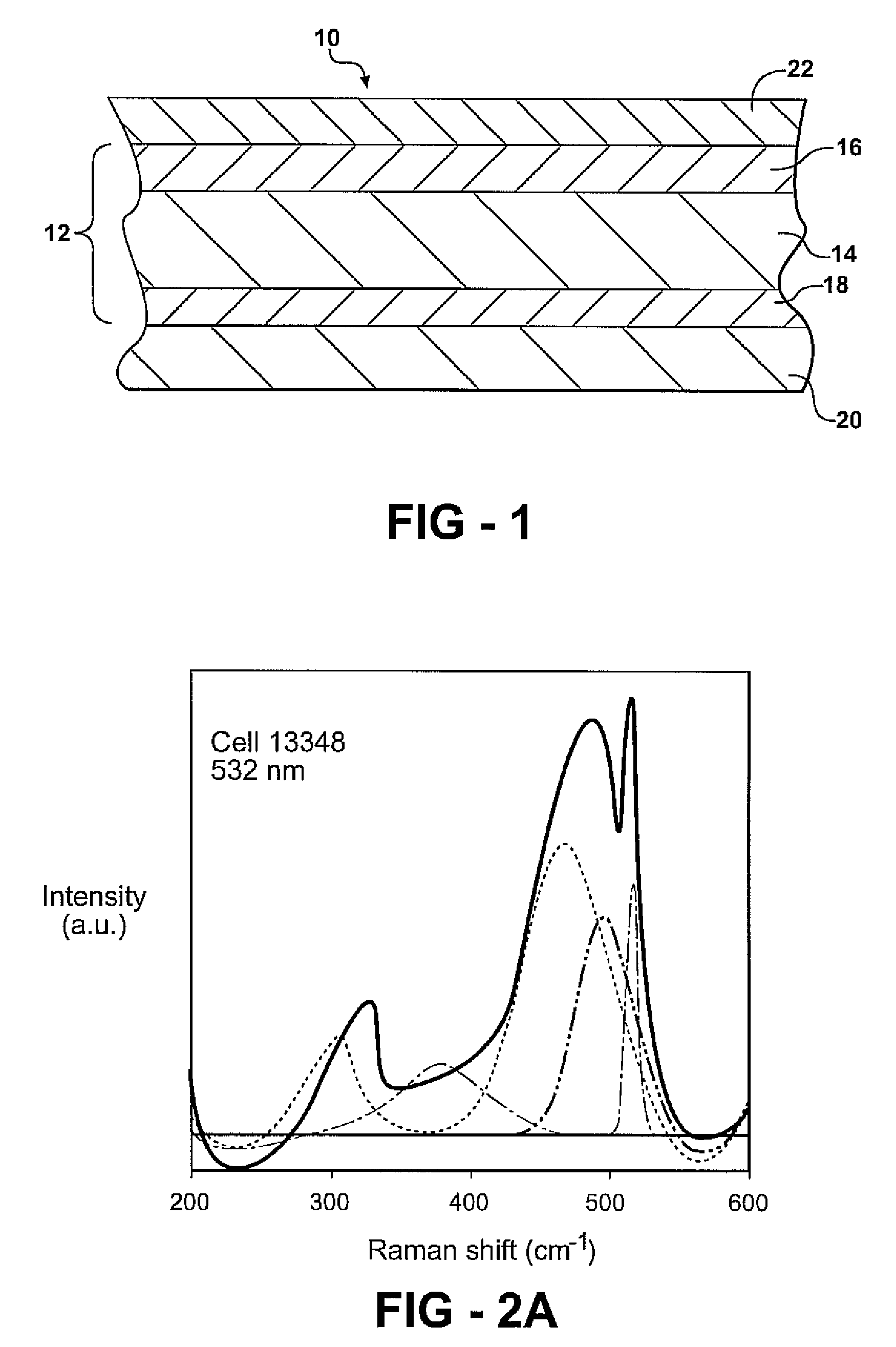
[0018]Referring now to FIG. 1, there is shown a p-i-n type photovoltaic device 10 of the type in which the present invention may be implemented. As is known in the art, photovoltaic devices of this type include at least one triad of semiconductor layers 12. This triad 12 is comprised of a layer of substantially intrinsic semiconductor material 14 interposed between a layer of p-doped semiconductor material 16 and a layer of n-doped semiconductor material 18. The photovoltaic device 10 further includes a support substrate 20. The substrate 20, as is known in the art, may comprise an electrically conductive body, such as a body of metal, and in that regard will function as an electrode of the photovoltaic device 10. The substrate 20 may also, in some instances, comprise an electrically insulating body such as a polymeric or glass member, having an electrically conductive layer of material thereupon. As is further known in the art, the substrate 20 may include additional layers such as...


PUM

PropertyMeasurementUnit
sizeaaaaaaaaaa
sizeaaaaaaaaaa
sizeaaaaaaaaaa

Abstract

A semiconductor device of p-i-n type configuration includes a p layer which is comprised of a p-doped semiconductor material, an n layer comprised of an n-doped semiconductor material and an i layer comprised of a substantially intrinsic, nanocrystalline semiconductor material interposed therebetween. The crystalline volume in the i layer decreases as the thickness of said layer increases from its interface with the n layer to its interface with the p layer. The grain size of the substantially intrinsic nanocrystalline semiconductor material may also decrease as the thickness of the i layer increases from its interface with the n layer to its interface with the p layer. The volume of regions of intermediate range order in a portion of the i layer commencing at the interface of the i layer and the p layer, and comprising no more than 50% of the thickness thereof, is greater than is the volume of regions of intermediate range order in the remainder of the i layer. Devices of this type may be used as photovoltaic devices, and may be fabricated by a plasma deposition process.

Description

CROSS-REFERENCE TO RELATED APPLICATIONS[0001]This application claims priority of U.S. Provisional Patent Application Ser. No. 60 / 798,547 filed May 8, 2006, entitled “Stabilized Photovoltaic Device and Methods for Its Manufacture”.FIELD OF THE INVENTION[0002]This invention generally relates to semiconductor devices. More specifically, the invention relates to photovoltaic devices. Most specifically, the invention relates to photovoltaic devices fabricated from nanocrystalline, hydrogenated semiconductor alloys, which devices exhibit enhanced performance and / or resistivity to photo degradation.BACKGROUND OF THE INVENTION[0003]Nanocrystalline materials provide for some specific advantages in the fabrication of semiconductor devices, such as photovoltaic devices. However, nanocrystalline materials have, heretofore, been poorly understood, and as a consequence, their potential has not always been realized in particular applications. It has been found that in certain applications, nanocry...

Claims


Application Information

Patent Timeline
Patent Type & Authority Applications(United States)
IPC IPC(8): H01L31/00
CPCB82Y10/00H01L31/075Y02E10/545H01L31/03685H01L31/03767Y02E10/548H01L31/0236H01L31/0352
Inventor GUHA, SUBHENDUYANG, CHIYAN, BAOJIEYUE, GUOZHEN
Owner UNITED SOLAR OVONIC
Why Eureka
Try Eureka