Nonvolatile semiconductor memory device and manufacturing method thereof

a semiconductor memory and non-volatile technology, applied in semiconductor devices, solid-state devices, instruments, etc., can solve the problems of low reliability of memory cells, achieve the effect of improving the reliability of flash memory, reducing the threshold voltage change, and reducing the number of errors

Inactive Publication Date: 2007-11-08
RENESAS TECH CORP
View PDF5 Cites 91 Cited by
  • Summary
  • Abstract
  • Description
  • Claims
  • Application Information

AI Technical Summary

Benefits of technology

[0014] An object of the present invention is to improve the reliability of a flash memory by decreasing the threshold voltage change caused by the change of potential (threshold voltage state) of a memory cell adjacent in a word line direction to reduce the miss-reading.

Problems solved by technology

As a result, in the memory cells, when reading data from a selected memory cell (for example, MC1), the threshold voltage shift applied to the memory cell (MC1) by the change of a threshold voltage state of an adjacent memory cell (for example, MC2) is rather increased, and problems which lower the reliability of the memory cells such as miss-reading occur.

Method used


Image

  • Nonvolatile semiconductor memory device and manufacturing method thereof
  • Nonvolatile semiconductor memory device and manufacturing method thereof
  • Nonvolatile semiconductor memory device and manufacturing method thereof

Examples


first embodiment

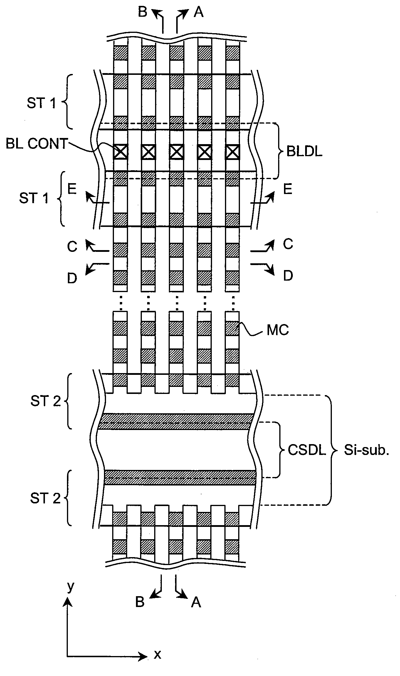
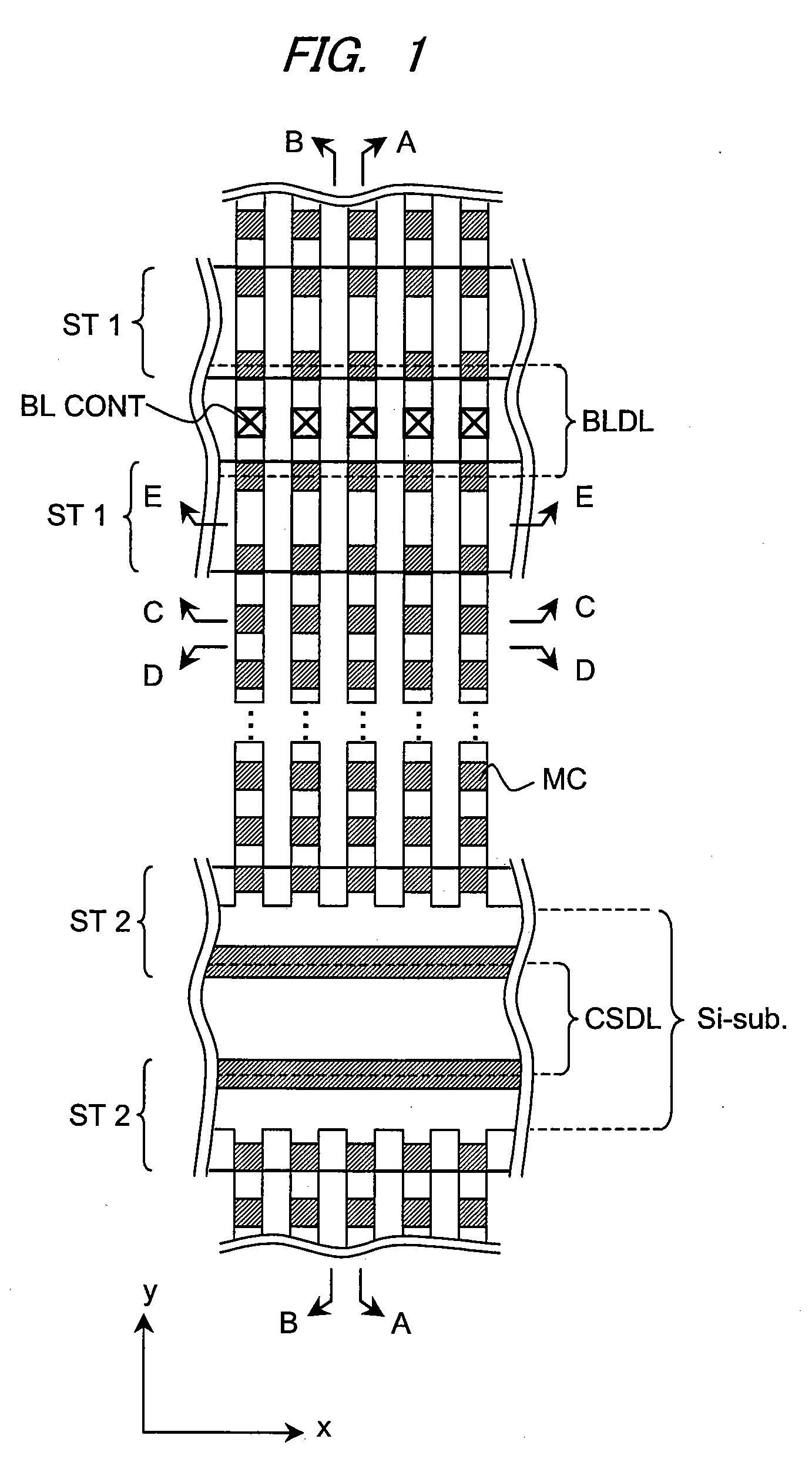
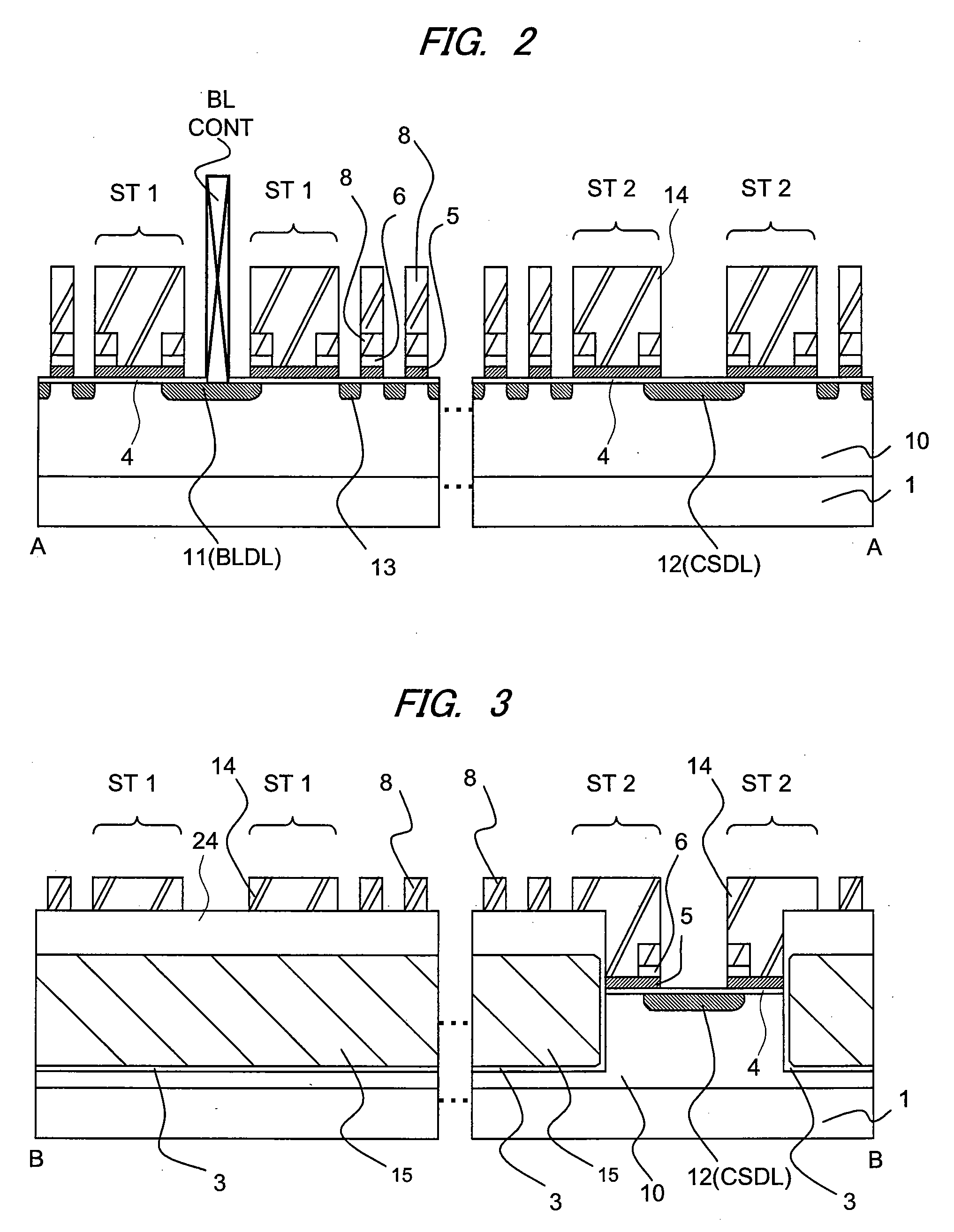
[0103]FIG. 1 is a plan view showing the principal part of a memory array region of a semiconductor device according to a first embodiment of the present invention, FIG. 2 to FIG. 6 are sectional views taken along the line A-A, the line B-B, the line C-C, the line D-D, and the line E-E in FIG. 1, respectively, and FIG. 7 to FIG. 9 are circuit diagrams for describing the operation of the semiconductor device according to the first embodiment of the present invention. In FIG. 1, the illustration of some members is omitted so as to make the structure of the memory array region easy to see.

[0104] The semiconductor device of this embodiment is a NAND type flash memory. Memory cells are formed on p-type wells 10 in a semiconductor substrate (hereinafter, referred to as substrate) 1 made of p-type single crystal silicon and include gate insulator films (tunnel insulator films) 4, floating gates 5, high-K insulator films 6, control gates 8, and n-type diffusion layers 13 (source, drain). Th...

second embodiment

[0127]FIG. 29 is a plan view showing the principal part of a memory array region of the semiconductor device according to a second embodiment, FIG. 30 to FIG. 34 are sectional views taken along the line A-A, the line B-B, the line C-C, the line D-D, and the line E-E in FIG. 29, respectively, and FIG. 35 to FIG. 37 are circuit diagrams for describing the operation of the semiconductor device according to the second embodiment. In FIG. 29, the illustration of some members is omitted so as to make the structure of the memory array region easy to see.

[0128] The semiconductor device of this embodiment is a flash memory. Memory cells are formed on p-type wells 10 in a semiconductor substrate 1 made of p-type single crystal silicon and include gate insulator films (tunnel insulator films) 4, floating gates 5, high-K insulator films 6, control gates 8, n-type diffusion layers 11 (drain), and n-type diffusion layers 12 (source). The control gates 8 extend in a row direction (x direction in ...

third embodiment

[0146]FIG. 53 is a plan view showing the principal part of a memory array region of a semiconductor device according to a third embodiment, FIG. 54 to FIG. 57 are sectional views taken along the line A-A, the line B-B, the line C-C, and the line D-D in FIG. 53, respectively, and FIG. 58 to FIG. 60 are circuit diagrams for describing the operation of the semiconductor device according to the third embodiment. In FIG. 53, the illustration of some members is omitted so as to make the structure of the memory array region easy to see.

[0147] The semiconductor device of this embodiment is a NAND type flash memory. Similar to the first embodiment, memory cells are formed on p-type wells 10 in a semiconductor substrate 1 and include gate insulator films (tunnel insulator films) 4, floating gates 5, high-K insulator films 6, control gates 8, and n-type diffusion layers 13 (source, drain). The control gates 8 extend in a row direction (x direction in FIG. 53) and form the word lines WL. The p...


PUM


Abstract

By decreasing the threshold voltage shift due to the potential change of the cells adjacent in a word line direction, the reliability of a flash memory can be enhanced. Memory cells of a flash memory are formed in p-type wells of a semiconductor substrate and include gate insulator films, floating gates, high-K insulator films, and control gates (word lines). The floating gates and control gates (word lines) are isolated by high-K insulator films. The plurality of memory cells arrayed in row a direction are isolated by isolation trenches extending in a column direction. In the isolation trenches, a silicon oxide film is embedded. In the silicon oxide film, an air gap is provided. A lower end of the air gap extends near to the bottom of the isolation trench, and its upper end extends further above the upper surface of the high-K insulator film covering the floating gate.

Description

CROSS-REFERENCE TO RELATED APPLICATION [0001] The present application claims priority from Japanese Patent Application No. JP 2006-127406 filed on May 1, 2006, the content of which is hereby incorporated by reference into this application. TECHNICAL FIELD OF THE INVENTION [0002] The present invention relates to a semiconductor device and a manufacturing method thereof. More particularly, it relates to a technology effectively applied to achieve the high integration density and performance improvement in a semiconductor device having an electrically programmable nonvolatile memory. BACKGROUND OF THE INVENTION [0003] Of the electrically programmable nonvolatile memories, a flash memory is known as the bulk erasable one. The flash memory is excellent in portability and impact resistance, and can be electrically erased in bulk. Therefore, its demand as a memory device for small portable information devices such as a mobile personal computer and a digital still camera has been rapidly ex...

Claims


Application Information

Patent Timeline
Patent Type & Authority Applications(United States)
IPC IPC(8): H01L29/788
CPCG11C16/0416G11C16/0483H01L27/11524H01L27/115H01L27/11521H01L21/764H10B69/00H10B41/35H10B41/30H10B63/80
Inventor SASAGO, YOSHITAKAISHI, TOMOYUKIMINE, TOSHIYUKIOSABE, TARO
Owner RENESAS TECH CORP
Why Eureka
Try Eureka