Method and system for fabricating a semiconductor device

a semiconductor and device technology, applied in the field of method and system for fabricating a semiconductor device, can solve the problems of high cost of such a fabrication apparatus, imperfect flip-chip connection, increased mounting cost of semiconductor chips, etc., and achieve the effect of perfect flip-chip connection and reduced fabrication cos

Inactive Publication Date: 2007-11-15
FUJITSU LTD
View PDF14 Cites 4 Cited by
  • Summary
  • Abstract
  • Description
  • Claims
  • Application Information

AI Technical Summary

Benefits of technology

[0015] It is an object of this invention to provide a method and a system for fabricating a semiconductor device, in which a fabrication apparatus cost and a fabrication cost may be reduced, and a perfect flip-chip connection may be performed, in which the disadvantages described above are eliminated.

Problems solved by technology

A cost of such a fabrication apparatus is high.
Therefore, by spending time for thermosetting the insulating adhesive 18 with the high-cost fabrication apparatus, there is thus a problem that a mounting cost of the semiconductor chip is increased.
However, a difference (about 4 times) in thermal expansion between the semiconductor chip and the substrate makes the flip-chip connection imperfect.

Method used


Image

  • Method and system for fabricating a semiconductor device
  • Method and system for fabricating a semiconductor device
  • Method and system for fabricating a semiconductor device

Examples


Embodiment Construction

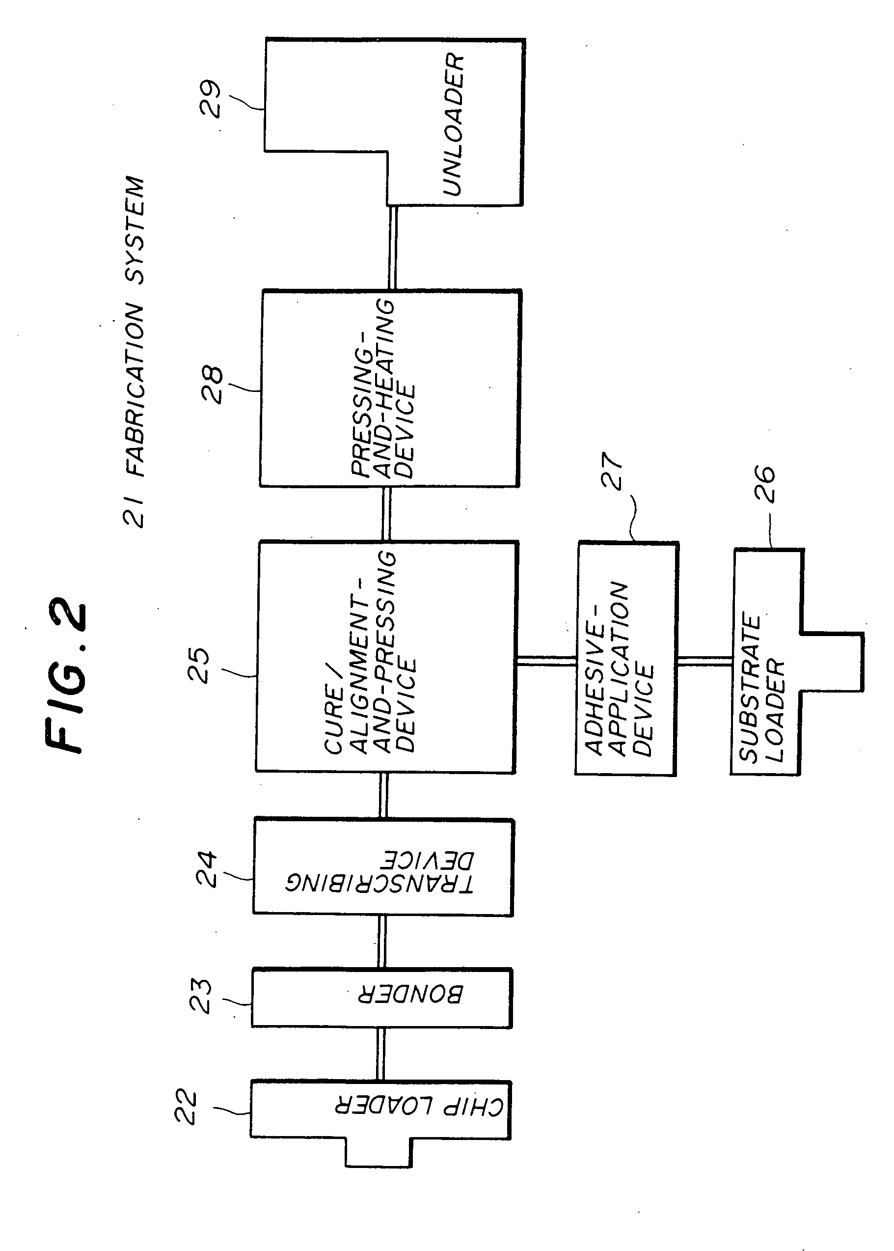
[0033] First, a description will be given of first embodiment of a fabrication method of a semiconductor device according to the present invention, by referring to FIG. 2. FIG. 2 shows an overall block diagram of a fabrication system 21 for realizing the fabrication method according to the present invention.

[0034] In the fabrication system shown in FIG. 2, a chip loader 22 supplies a semiconductor chip on which a given number of electrode pads (e.g. aluminum pads) are formed, and a bonder 23 forms stud-bumps as projection electrodes on the semiconductor chip by means of a wire-bonding technology.

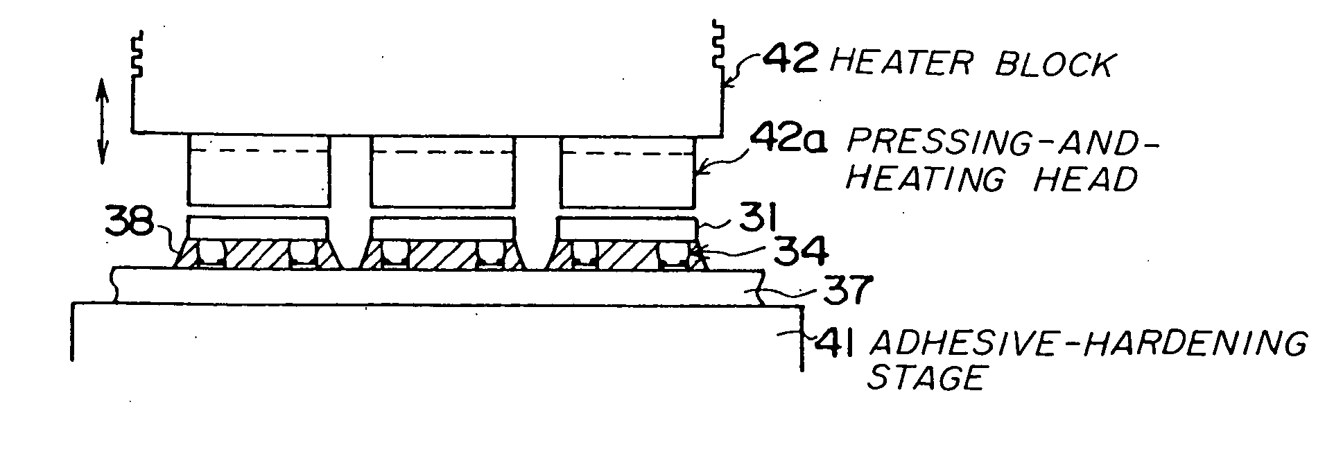
[0035] A transcribing device 24 transcribes a conductive adhesive on a surface of the stud-bumps. A cure / alignment-and-pressing device 25 heats a substrate with an adhesive-half-thermosetting temperature, and aligns the semiconductor chip, on which stud-bumps are formed, to the substrate by a stepper to perform a first fixing with a first pressure.

[0036] A substrate loader 26 supplies the...


PUM

PropertyMeasurementUnit
heightsaaaaaaaaaa
heightaaaaaaaaaa
insulatingaaaaaaaaaa

Abstract

A fabrication method of a semiconductor device is disclosed. The method includes the following steps. First, a given number of projection electrodes are formed on each of a given number of semiconductor chips, and a thermosetting insulating adhesive is applied to areas of mounting parts where the semiconductor chips are to be mounted on a substrate. Second, the thermosetting insulating adhesive on the substrate is heated with a half-thermosetting temperature. Third, the semiconductor chips are aligned to the mounting parts of the substrate and a first fixing of the semiconductor chips is performed with a first pressure. Fourth, the substrate, on which the semiconductor chips are fixed, is heated with a thermosetting temperature of the thermosetting insulating adhesive, and a second fixing of the semiconductor chips is performed with a second pressure.

Description

BACKGROUND OF THE INVENTION [0001] 1. Field of the Invention [0002] The present invention generally relates to a method and a system for fabricating a semiconductor device, and more particularly, to a method and a system for fabricating a semiconductor device, in which a flip-chip connection is performed. [0003] Recently, according to a progress of a high-density integration of the semiconductor device, the flip-chip connection with bumps is frequently used to perform a high-density mounting of a semiconductor chip and to shorten a length of routing lines for requirement of a fast operation. Further, such a semiconductor device has to be fabricated with a low cost. To meet the above requirements, it is necessary to achieve a considerably precise alignment in the mounting of the semiconductor chip with the low cost. [0004] 2. Description of the Prior Art [0005]FIGS. 1A to 1E show illustrations for explaining fabrication procedures of a conventional flip-chip-type semiconductor device...

Claims


Application Information

Patent Timeline
Patent Type & Authority Applications(United States)
IPC IPC(8): B23P19/00H01L21/60
CPCH01L21/6835H01L24/11H01L24/83H01L24/90H01L24/95H01L25/50H01L2224/1134H01L2224/13099H01L2224/13124H01L2224/13144H01L2224/13147H01L2224/16225H01L2224/73204H01L2224/75251H01L2224/75252H01L2224/78302H01L2224/83191H01L2224/83192H01L2224/83194H01L2224/83855H01L2224/83856H01L2924/01004H01L2924/01005H01L2924/01013H01L2924/01029H01L2924/01079H01L2924/0781H01L2924/01006H01L2924/01033H01L24/29H01L2224/32225H01L2224/45147H01L2224/11822H01L2224/45144H01L2224/45124H01L2924/00014H01L2924/07802Y10T29/53178Y10T29/53191Y10T29/53187H01L2924/00H01L2924/00012H01L2224/81907H01L2224/48
Inventor KIRA, HIDEHIKOFUJII, MASANAOISHIKAWA, NAOKI
Owner FUJITSU LTD
Why Eureka
Try Eureka