Bolometric Infrared Sensor Having Two-Layer Structure and Method for Manufacturing the Same
- Summary
- Abstract
- Description
- Claims
- Application Information
AI Technical Summary
Benefits of technology
Problems solved by technology
Method used
Image
Examples
Embodiment Construction
[0033] Reference will now be made in detail to the preferred embodiments of the present invention, examples of which are illustrated in the accompanying drawings.
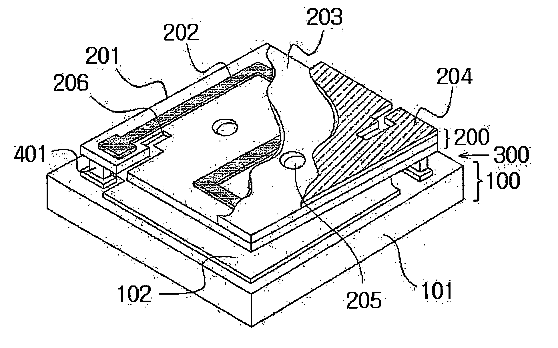
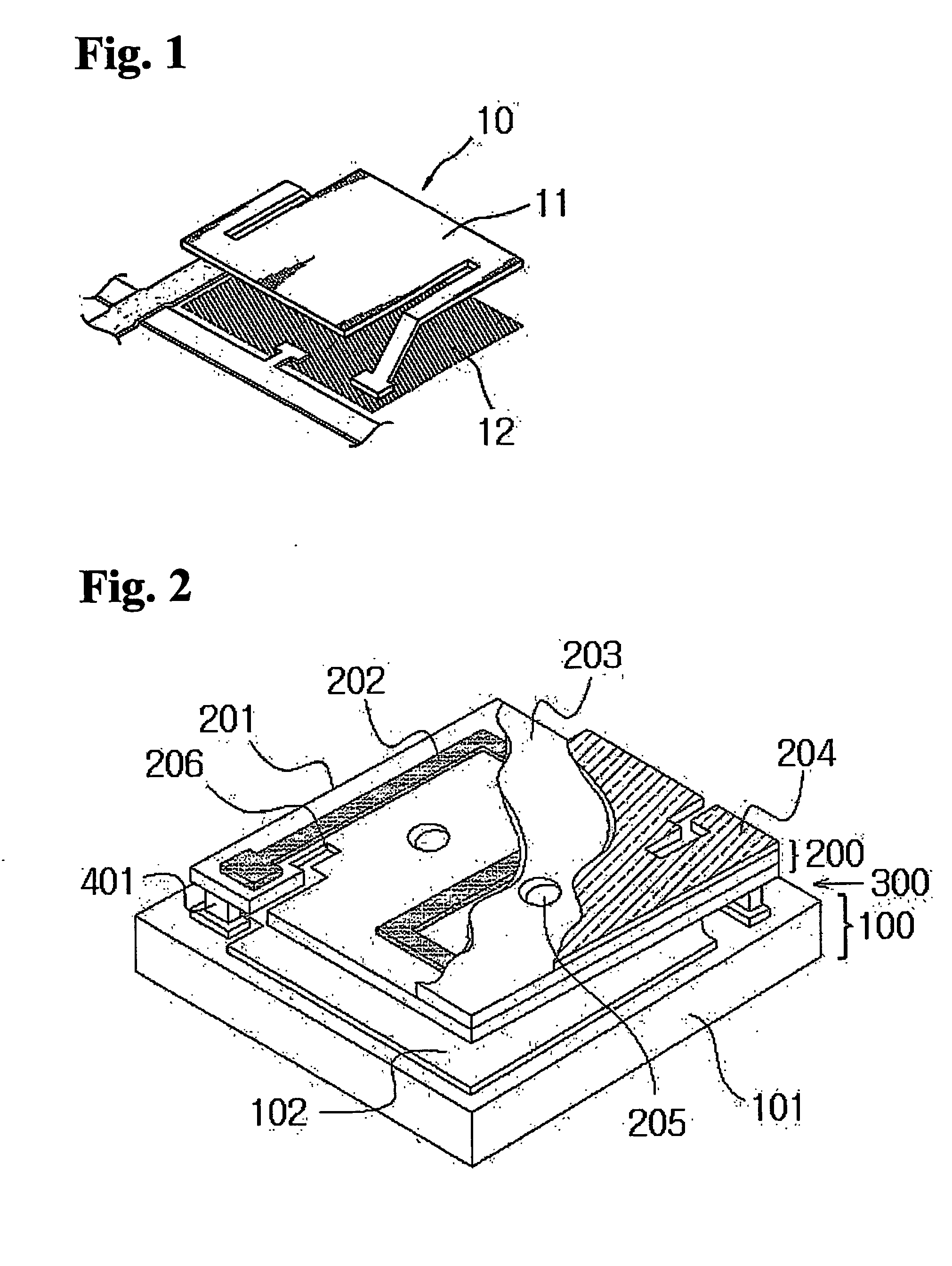
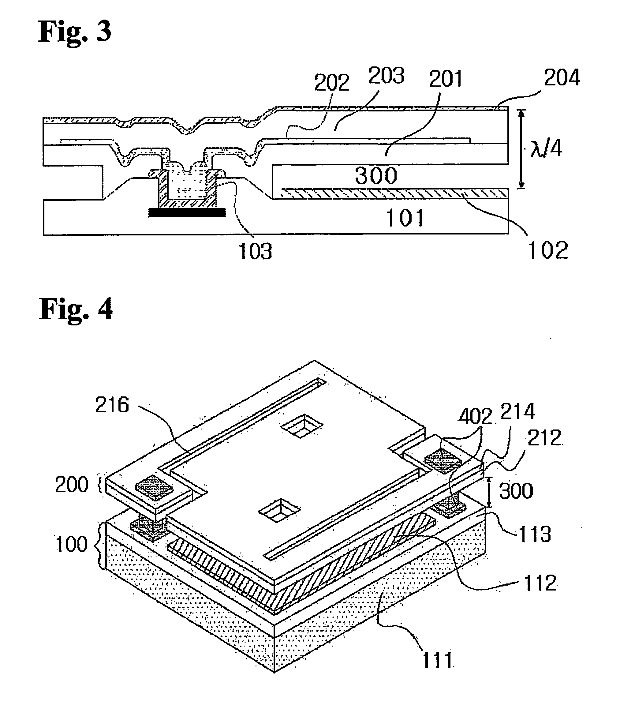
[0034]FIGS. 2 through 11 illustrate prospective, cross-sectional, and top views of unit pixels of a bolometric infrared sensor having a two-layer structure in accordance with embodiments of the present invention.
[0035] In accordance with the present invention, the IR sensor having a two-layer structure and unit pixel of 50 μm×50 μm comprises a bottom layer 100, an upper layer 200, a cavity therebetween 300, and anchors 401, 402, 403, 404a, 404b, 404c, 404d and 405 for supporting the upper layer 200.
[0036] The bottom layer 100 includes ROIC substrates 101, 111, 121, 131 and 141 (hereinafter collectively referred to as “1X1”) and reflective metal layers 102, 112, 132, and 142 (hereinafter collectively referred to as “1X2”) thereon. The reflective metal layers 1X2 are made of a material selected from the group consisting of...
PUM
 Abstract
Description
Claims
Application Information


