Plasma CVD apparatus equipped with plasma blocking insulation plate

a technology of plasma blocking and plasma cvd, which is applied in the field of single-wavefer processing of plasma cvd apparatus, can solve the problems of not meeting film quality and other requirements, reducing the floating potential, and not sufficiently adjusting the plasma processing conditions, so as to reduce the occurrence of plasma charging damage and pickup problems, the floating potential is low

Inactive Publication Date: 2007-11-22
ASM JAPAN
View PDF5 Cites 341 Cited by
  • Summary
  • Abstract
  • Description
  • Claims
  • Application Information

AI Technical Summary

Benefits of technology

[0013]This way, the area in which plasma generates can be limited. Through various other embodiments, the present invention also prevents plasma from coming in contact with the side faces of the heating block, interior walls of the reactor and other locations where conductive members are exposed, which consequently results in a lower floating potential applied to the processing target. As a result, occurrences of charging damage caused by plasma and pickup problem can be reduced.

Problems solved by technology

However, in many cases adjusting the plasma processing conditions is not sufficiently effective, and reducing the floating potential using this method also presents a number of problems such as the film quality and other requirements not being satisfied.
However, these technologies are not intended to reduce the floating potential, but they have other objects such as preventing contamination.
Also, covering the interior walls of the reactor with an insulation material requires major changes to the apparatus structure and this method is not applicable to current apparatuses.

Method used


Image

  • Plasma CVD apparatus equipped with plasma blocking insulation plate
  • Plasma CVD apparatus equipped with plasma blocking insulation plate
  • Plasma CVD apparatus equipped with plasma blocking insulation plate

Examples


example 1

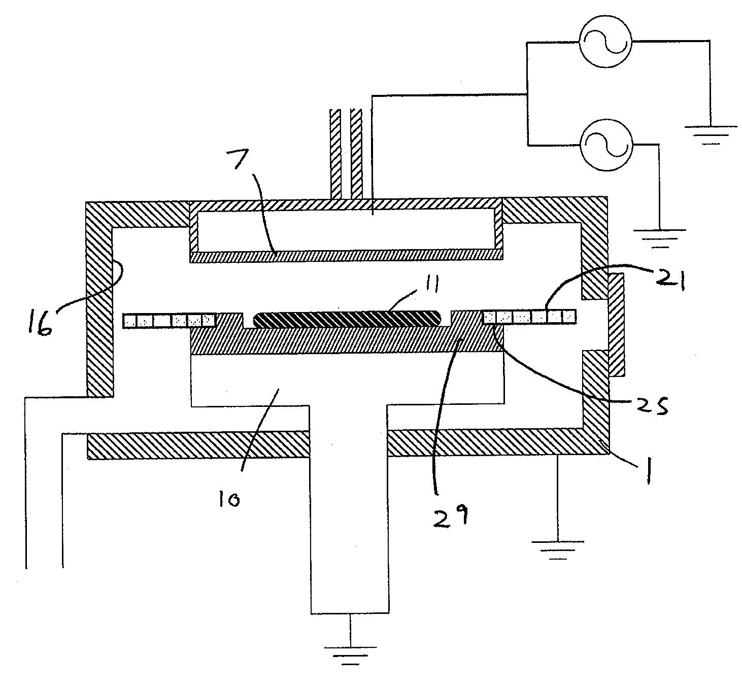
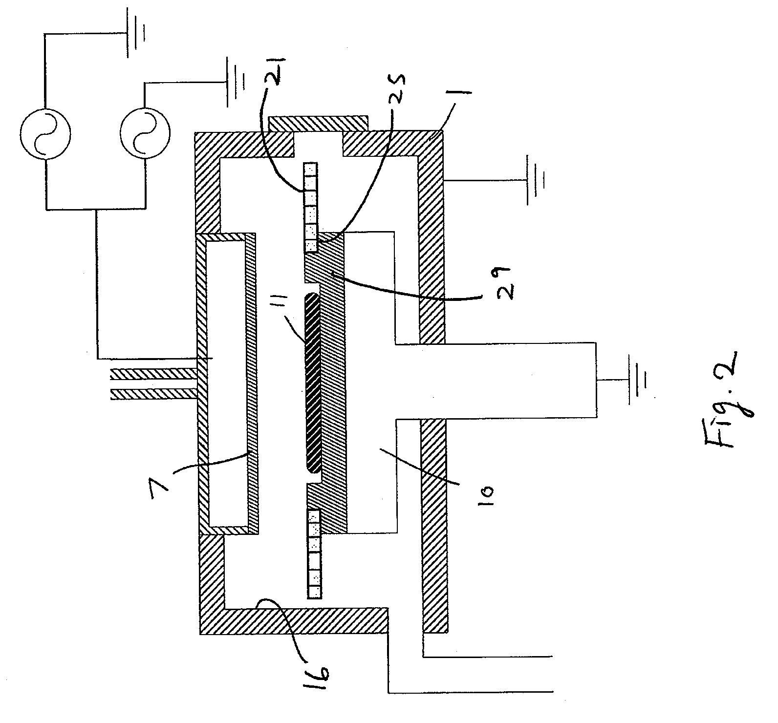
[0072]FIG. 2 shows the best mode of embodiment 1. In this example, an insulation plate 21 is placed on the susceptor 15 and moves together with the susceptor 15, as shown in FIG. 2.

[0073]The insulation plate 21 comprises a ceramic disc whose thickness is in a range of approx. 1 mm to approx. 10 mm (or preferably in a range of 1 mm to 5 mm, or more preferably in a range of 2 mm to 4 mm), and whose inner diameter is greater than the semiconductor substrate 11 while whose outer diameter is equal to or greater than 95% of the distance from a top plate 29 to an interior wall 16. In other words, the insulation plate must not contact the semiconductor substrate 11, and its inner diameter must be smaller than the semiconductor substrate 11 so that the insulation plate will not overlap with the semiconductor substrate 11. FIG. 10(b) shows a cross-section BB of the structure shown in FIG. 10(a). The gap between the substrate 11 and a lip 27 is not shown. The insulator 21 is attached to the ou...

example 2

[0090]In Example 2, the insulation plate is affixed. As shown in FIG. 7, an insulator 71 is affixed on a support 72 at the bottom of the reactor 1 so that its position aligns with the height of the bottom edge of the top plate (i.e., the insulator is positioned in a manner preventing the heating block 10 from being exposed).

[0091]Here, the insulator 71 may preferably be set above the bottom face of the heating block 10. FIG. 13 shows an example where an insulator 120 is arranged below the bottom face of a heating block 101. According to this structure, plasma enters the space between the heating block 101 and insulator 120, which is undesirable.

[0092]Desirably the gap between the susceptor and insulator may be minimized. Even when the insulator is affixed to the bottom of the reactor, the gap from the susceptor may preferably be kept to 2 mm or less.

[0093]The inner diameter of the insulation plate 71 is roughly the same as the outer diameter of the susceptor, while the outer diamete...

example 3

[0099]In Example 3, multiple insulation plates are used. FIG. 8 shows one example of this configuration. This configuration is characterized by setting two or more of the insulation plate shown in Example 1 and Example 2. A desired pattern of combination or number of insulation plates can be selected according to the apparatus.

[0100]In FIG. 8, one insulation plate 81 (movable insulation plate) is affixed onto the susceptor (top plate 89), while another insulation plate 83 (fixed insulation plate) is affixed onto the reactor 1. The two insulation plates are respectively set in positions where the insulation plates will not contact each other even when the susceptor moves up and down. Here, the movable insulation plate is positioned above, while the fixed insulation plate is positioned below. Accordingly, having a slight gap between the susceptor and fixed insulation plate positioned below will not present any problem because plasma can be shielded by the movable insulation plate posi...


PUM

PropertyMeasurementUnit
diameteraaaaaaaaaa
diameteraaaaaaaaaa
diameteraaaaaaaaaa

Abstract

A plasma CVD apparatus for forming a thin film on a substrate includes: a vacuum chamber; an upper electrode; a susceptor as a lower electrode; and a ring-shaped insulation plate disposed in a gap between the susceptor and an inner wall of the chamber in the vicinity of or in contact with the susceptor to minimize a floating potential charged on the substrate while processing the substrate.

Description

CROSS-REFERENCE TO RELATED APPLICATIONS [0001]This application claims the benefit of U.S. Provisional Application No. 60 / 800,670, filed May 16, 2006, the disclosure of which is herein incorporated by reference in its entirety.BACKGROUND OF THE INVENTION [0002]1. Field of the Invention[0003]The present invention generally relates to a plasma CVD apparatus, particularly to a single-wafer processing plasma CVD apparatus.[0004]2. Description of the Related Art[0005]On manufacturing lines using semiconductor apparatuses, dry etching, plasma CVD and other plasma processes are widely used. The plasma CVD apparatus shown in FIG. 1 is one example of the apparatus used to implement these plasma processes. This plasma CVD apparatus for forming a film on a semiconductor substrate 11 comprises a reactor chamber 1, a susceptor 15 (with a top plate 9 and a heating block 10) located in the reactor chamber 1 and used to place the semiconductor substrate 11 on top, a showerhead 7 facing the susceptor...

Claims


Application Information

Patent Timeline
Patent Type & Authority Applications(United States)
IPC IPC(8): H05H1/24C23C16/00
CPCC23C16/4585C23C16/5096H01J37/32642H01J37/32623H01J37/32091
Inventor SHUTO, MITSUTOSHIFUKASAWA, YASUSHINAKANO, RYUSUZUKI, YASUAKI
Owner ASM JAPAN
Why Eureka
Try Eureka