Semiconductor device having improved insulated gate bipolar transistor and method for manufacturing the same

a technology of insulated gate bipolar transistor and semiconductor device, which is applied in the direction of semiconductor device, electrical apparatus, transistor, etc., can solve the problems of insufficient reduction of on-voltage, and achieve the effect of suppressing power loss in turnoff and reducing on-voltag

Inactive Publication Date: 2007-11-22
MITSUBISHI ELECTRIC CORP
View PDF4 Cites 67 Cited by
  • Summary
  • Abstract
  • Description
  • Claims
  • Application Information

AI Technical Summary

Benefits of technology

[0009]The present invention has been developed to solve the above-described problems, and therefore it is an object of the present invention to provide an insulated gate semiconductor device that can reduce the on-voltage between the collector and the emitter while suppressing the power loss in turnoff, and a method for manufacturing such an insulated gate semiconductor device.

Problems solved by technology

Therefore, there was a problem wherein the thickness of the portion of the carrier stored layer having high impurity concentration was thinned, and the on-voltage could not be sufficiently reduced.

Method used


Image

  • Semiconductor device having improved insulated gate bipolar transistor and method for manufacturing the same
  • Semiconductor device having improved insulated gate bipolar transistor and method for manufacturing the same
  • Semiconductor device having improved insulated gate bipolar transistor and method for manufacturing the same

Examples


first embodiment

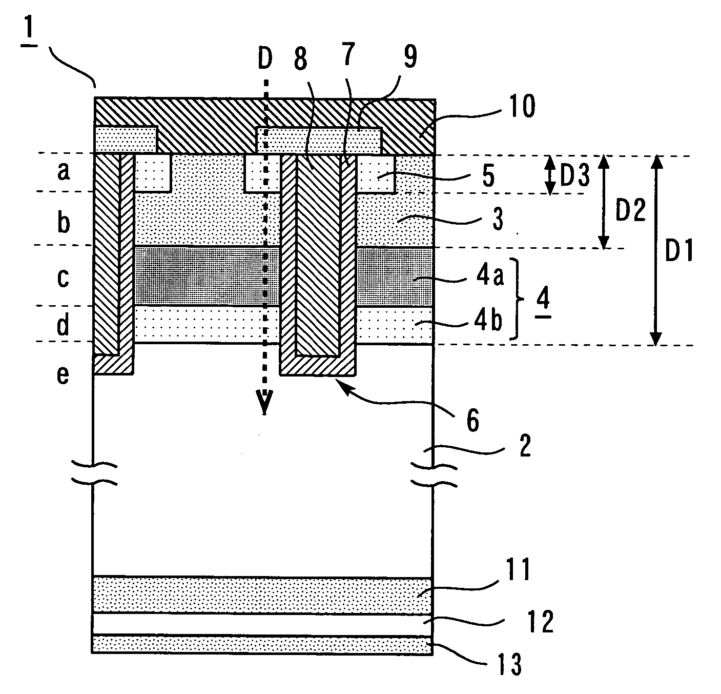
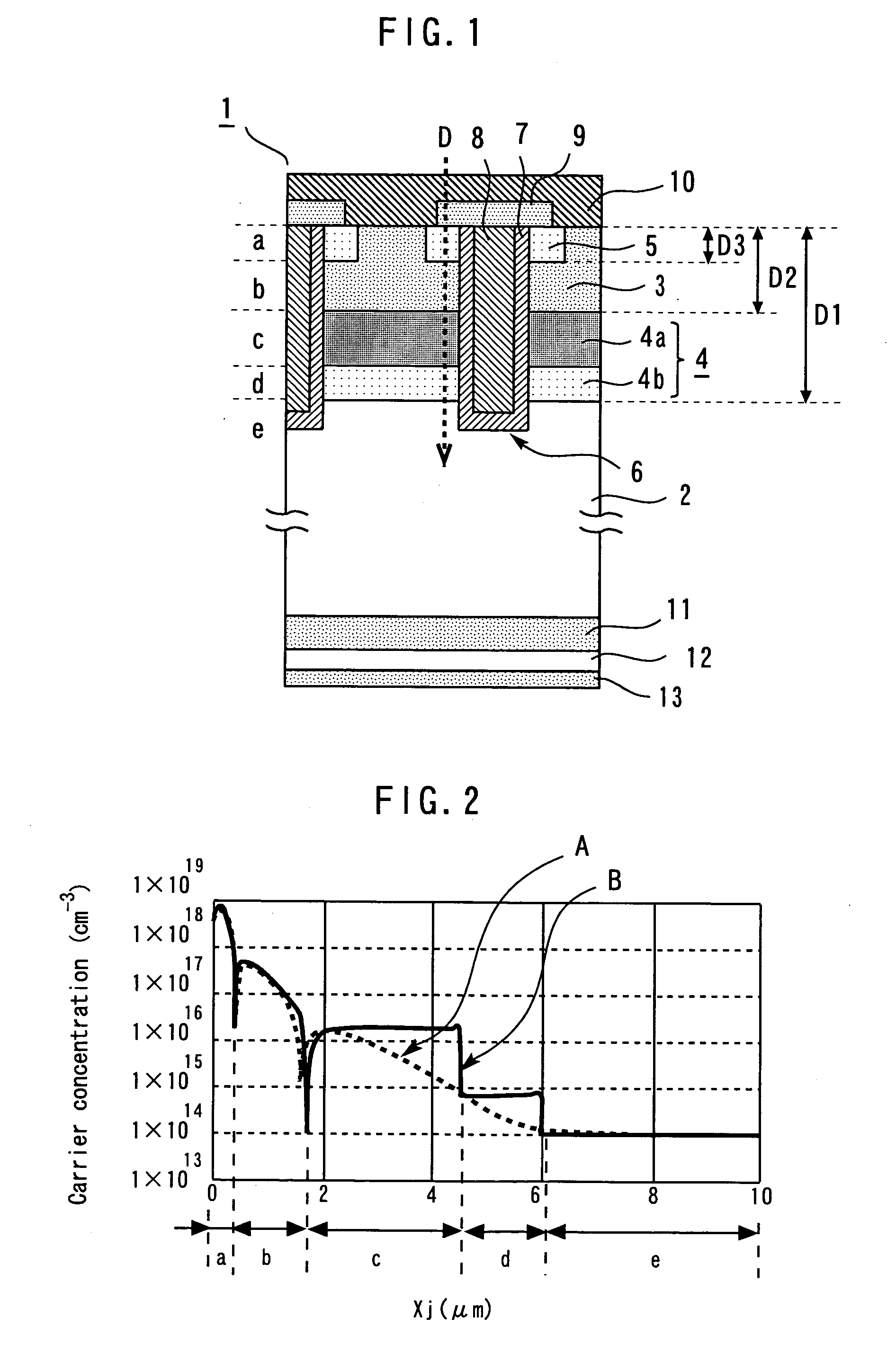
[0021]An insulated gate semiconductor device according to the first embodiment will be described referring to FIG. 1. The semiconductor device has an insulated gate bipolar transistor (hereafter abbreviated as “IGBT”) of a trench type. The semiconductor device is formed using a semiconductor substrate 1 having a first major surface (upper major surface) and a second major surface (lower major surface), and between the first major surface and the second major surface of the semiconductor substrate 1, an n-type (first conductivity type) first base layer 2 containing an n-type impurity is formed. On the first major surface of the semiconductor substrate 1, a p-type (second conductivity type) second base layer 3 is formed. Between the first base layer 2 and the second base layer 3 of the semiconductor substrate 1, a carrier stored layer 4 is formed. The carrier stored layer 4 has a n-type high-concentration impurity layer 4a having a higher impurity concentration than the first base lay...

second embodiment

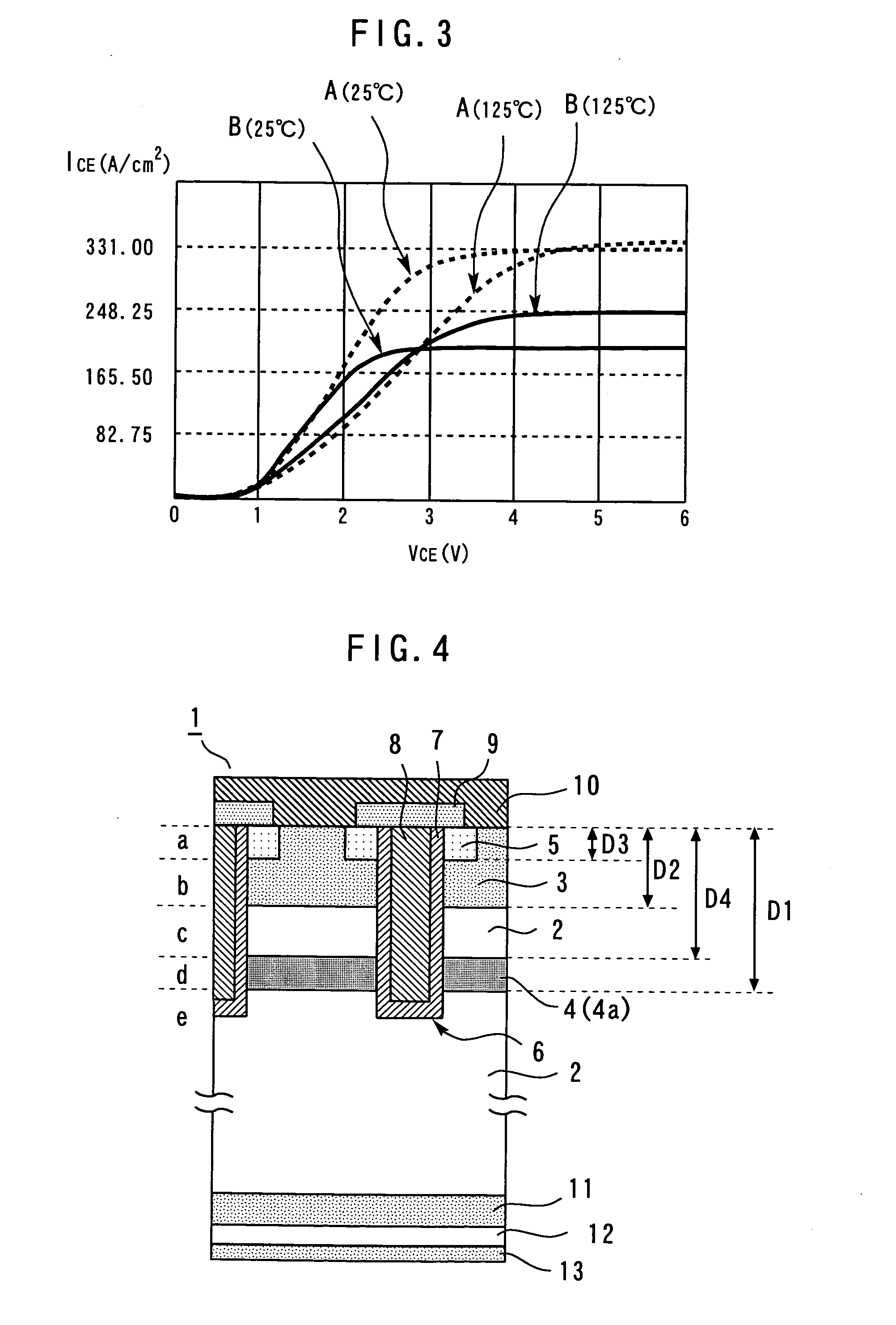
[0046]An insulated gate semiconductor device according to the second embodiment will be described referring to FIG. 4. Here, the description will be focused around aspects different from those in FIG. 1 in the first embodiment. The semiconductor device according to the first embodiment shown in FIG. 1 has a structure wherein a high-concentration impurity layer 4a is formed in the location c of the semiconductor substrate 1, and a low concentration impurity layer 4b is formed in the location d. Whereas the semiconductor device according to the second embodiment shown in FIG. 4 has a structure wherein a carrier stored layer 4 composed of only a high-concentration impurity layer 4a is formed under the second base layer 3 apart from the second base layer 3 by a predetermined distance (D4-D2). Specifically, the semiconductor device shown in the second embodiment has a structure wherein the high-concentration impurity layer 4a of the carrier stored layer 4 is formed under the second base ...


PUM


Abstract

An n-type first base layer is formed on a semiconductor substrate 1 having a first major surface and a second major surface, and a p-type second base layer is formed thereon. Between the first base layer and the second base layer, a carrier stored layer is formed. The carrier stored layer has a high-concentration impurity layer and a low concentration impurity layer, and the high-concentration impurity layer has a thickness of 1.5 μm or more and an impurity concentration therethrough is made to be 1.0×1016 cm−3 or more throughout the layer.

Description

BACKGROUND OF THE INVENTION[0001]1. Field of the Invention[0002]The present invention relates to a semiconductor device and a method for manufacturing the same, and specifically to an insulated gate semiconductor device having an insulated gate bipolar transistor and a method for manufacturing the same.[0003]2. Background Art[0004]In a power semiconductor element, an insulated gate bipolar transistor (hereafter abbreviated as “IGBT”) having a trench structure is widely used as a switching element. An example of IGBT structures will be described below.[0005]An n-type base layer is formed between a first major surface and a second major surface of a semiconductor substrate, and a p-type base layer is formed on the first major surface side of the n-type base layer. In the p-type base layer, an n-type emitter layer is selectively formed. A trench is formed extending through the n-type emitter layer and the p-type base layer, and an insulating film is formed along the inner surface there...

Claims


Application Information

Patent Timeline
Patent Type & Authority Applications(United States)
IPC IPC(8): H01L29/76
CPCH01L29/0834H01L29/7397H01L29/0847H01L29/73
Inventor HARADA, TATSUO
Owner MITSUBISHI ELECTRIC CORP
Why Eureka
Try Eureka