GaN hetero-junction diode device and method for manufacturing same

A heterojunction and diode technology, applied in semiconductor/solid-state device manufacturing, semiconductor devices, electrical components, etc., can solve problems such as increased leakage, achieve low turn-on voltage, high forward conduction current, and solve conflicting effects

Active Publication Date: 2015-02-18
GPOWER SEMICON
View PDF6 Cites 22 Cited by
  • Summary
  • Abstract
  • Description
  • Claims
  • Application Information

AI Technical Summary

Problems solved by technology

If you want to reduce the turn-on voltage, you need to reduce the Schottky barrier, but the leakage will increase when the reverse bias is applied, so there is a contradictory relationship between the forward turn-on voltage and the reverse leakage

Method used


Image

  • GaN hetero-junction diode device and method for manufacturing same
  • GaN hetero-junction diode device and method for manufacturing same
  • GaN hetero-junction diode device and method for manufacturing same

Examples


Embodiment 1

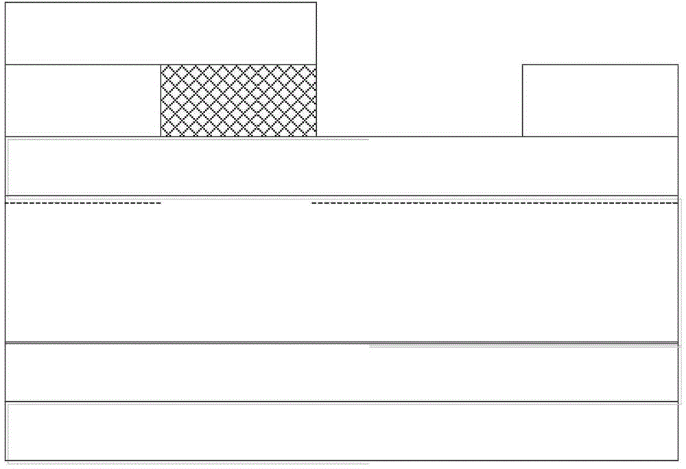
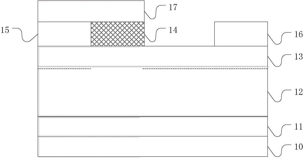
[0050] figure 2 It is a schematic structural diagram of a GaN heterojunction diode device provided in Embodiment 1 of the present invention. Such as figure 2 As shown, the GaN heterojunction diode device described in the embodiment of the present invention includes: a substrate 10, a buffer layer 11 on the substrate 10, a channel layer 12 on the buffer layer 11, and a barrier layer on the channel layer 12. Layer 13, the risk layer 14 on the potential barrier layer 13, the first ohmic anode 15 and the ohmic cathode 16 on both sides of the barrier layer 13 and the risk layer 14, the first ohmic anode is in contact with the risk layer, The second ohmic anode 17 is located on the first ohmic anode 15 and the ohmic layer 14, and the second ohmic anode is in contact with the ohmic metal of the ohmic layer.

[0051] Wherein, the substrate 10 may be silicon carbide, silicon or sapphire.

[0052] The material of the buffer layer 11 can be non-doped GaN, AlN or other III-V nitrides...

Embodiment 2

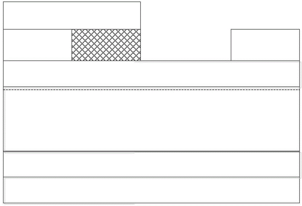
[0072] The GaN heterojunction diode device provided in Embodiment 2 of the invention is based on the GaN heterojunction diode device in Embodiment 1 above, and the difference from Embodiment 1 is that the GaN heterojunction diode device provided in Embodiment 2 is The layer adopts p-type GaN with a thickness of 10-200nm. The advantage of choosing p-type GaN as the capping layer of the GaN heterojunction diode is that a selective etching method can be used in the preparation process, so that the etching of the capping layer can accurately stay on the AlGaN barrier layer.

[0073] Figure 4 It is a schematic structural diagram of a GaN heterojunction diode device provided in Embodiment 2 of the present invention. Such as Figure 4 As shown, the GaN heterojunction diode device described in the embodiment of the present invention includes: a substrate 20, a buffer layer 21 on the substrate 20, a channel layer 22 on the buffer layer 21, and a barrier layer on the channel layer 22...

Embodiment example 3

[0091] The GaN heterojunction diode device provided in Embodiment 3 of the present invention is based on the GaN heterojunction diode device in Embodiment 2 above. The difference from Embodiment 2 is that the GaN heterojunction diode device provided in Embodiment 3 has The first ohmic anode, ohmic cathode, and second ohmic anode are prepared at one time, and the anode and cathode electrode structures are any one or any combination of Ni, Au, Pt, Pd, W, Ag, Cr, ITO alloy. In this embodiment, the first ohmic anode and the second ohmic anode are collectively referred to as ohmic anodes.

[0092] Figure 6 is a schematic structural diagram of a GaN heterojunction diode device provided in Embodiment 3 of the present invention, as shown in Figure 6 As shown, the GaN heterojunction diode device includes: a substrate: 30, a buffer layer 31 on the substrate 30, a channel layer 32 on the buffer layer 31, a barrier layer 33 on the channel layer 32, A layer 34 on the barrier layer 33,...


PUM


Abstract

The invention discloses a GaN hetero-junction diode device and a method for manufacturing the same. The GaN hetero-junction diode device comprises a substrate, a buffer layer, a channel layer, a potential barrier layer, a cap layer, a first Ohm anode, an Ohm cathode and a second Ohm anode. The buffer layer is positioned on the substrate; the channel layer is positioned on the buffer layer; the potential barrier layer is positioned on the channel layer, the potential barrier layer and the channel layer form a hetero-structure, and a two-dimensional electric channel is formed at a hetero-junction interface; the cap layer is positioned on the potential barrier layer; the first Ohm anode and the Ohm cathode are positioned on the upper side of the potential barrier layer and are arranged on two sides of the cap layer, and the first Ohm anode is in contact with the cap layer; the second Ohm anode is positioned on the first Ohm anode and the cap layer and is in Ohm metal contact with the cap layer. The GaN hetero-junction diode device and the method have the advantages that the problem of conflict between forward start voltage control and reverse electric leakage in the prior art can be solved, and a diode has characteristics of low start voltages and turn-on resistance and high reverse withstand voltages and forward turn-on currents.

Description

technical field [0001] The invention relates to the technical field of semiconductors, in particular to a GaN heterojunction diode device and a manufacturing method thereof. Background technique [0002] The third-generation semiconductor gallium nitride (GaN) is a material with wide band gap, high thermal conductivity, high electron mobility and other properties. The high temperature, high voltage, high frequency and high power performance of GaN-based power devices are much higher than The first generation semiconductor silicon (Si) and the second generation semiconductor gallium arsenide (GaAs) material devices. At the same time, gallium nitride can form a heterojunction with other III-V compound semiconductors such as AlGaN. This structure has strong spontaneous polarization and piezoelectric polarization effects, and can form a high concentration of electrons near the interface of the heterojunction. The two-dimensional electron gas channel (2DEG), the density can reac...

Claims


Application Information

Patent Timeline
Patent Type & Authority Applications(China)
IPC IPC(8): H01L29/861H01L29/06H01L21/329
CPCH01L29/0611H01L29/66136H01L29/8611
Inventor 裴轶陈洪维
Owner GPOWER SEMICON
Why Eureka
Try Eureka