Gallium nitride diode and manufacturing method thereof

A manufacturing method and diode technology, applied in semiconductor/solid-state device manufacturing, semiconductor devices, electrical components, etc., can solve the problems of reduced Schottky barrier height, increased leakage, and increased leakage, achieving low turn-on voltage, low Effects of reverse leakage and low on-resistance

Active Publication Date: 2019-03-12
GPOWER SEMICON
View PDF4 Cites 0 Cited by
  • Summary
  • Abstract
  • Description
  • Claims
  • Application Information

AI Technical Summary

Problems solved by technology

If you want to reduce the forward turn-on voltage, you need to reduce the Schottky barrier, but after the Schottky barrier is reduced, when the diode is applied with a reverse bias, the leakage will increase, and there will be an image force effect Resulting in lower Schottky barrier height and increased leakage

Method used


Image

  • Gallium nitride diode and manufacturing method thereof
  • Gallium nitride diode and manufacturing method thereof
  • Gallium nitride diode and manufacturing method thereof

Examples


Embodiment 1

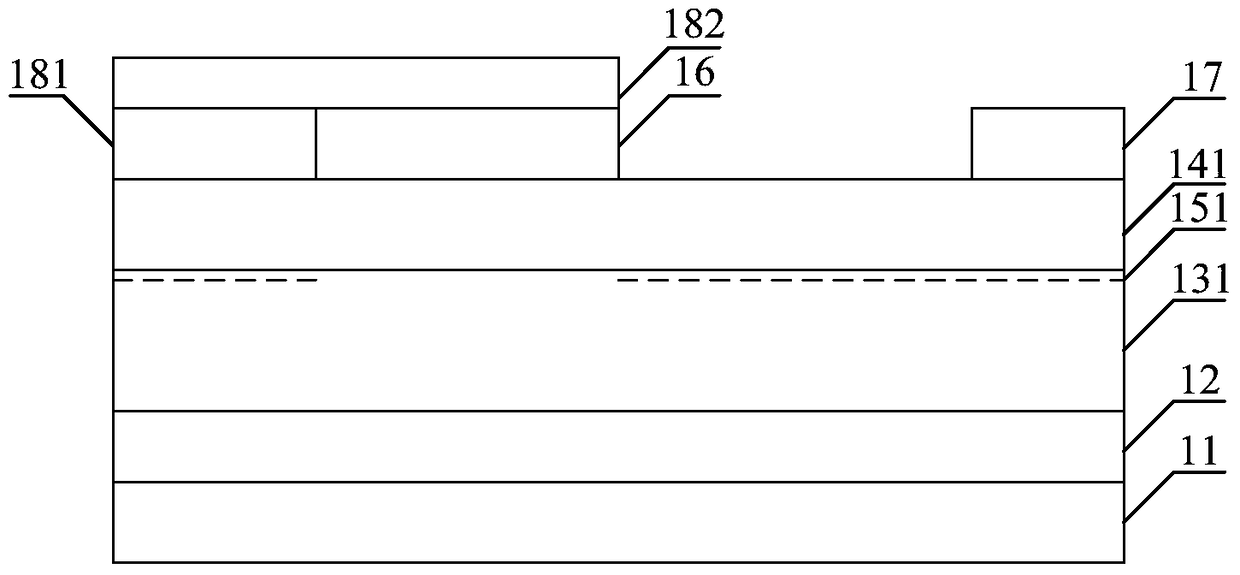
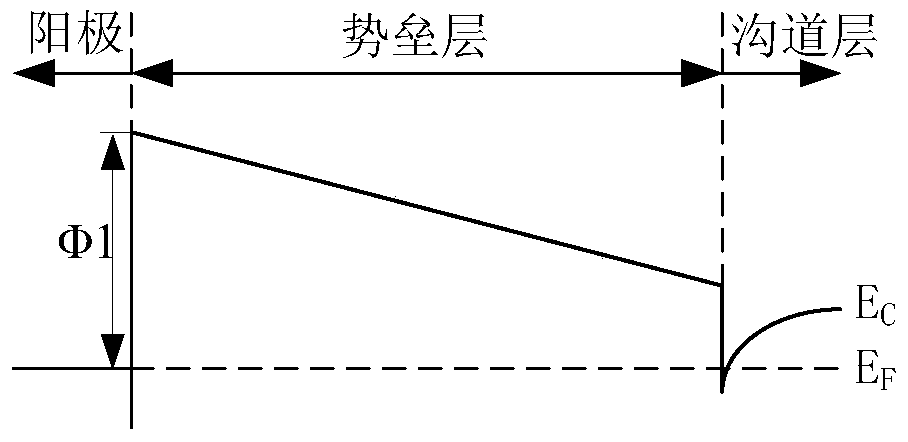
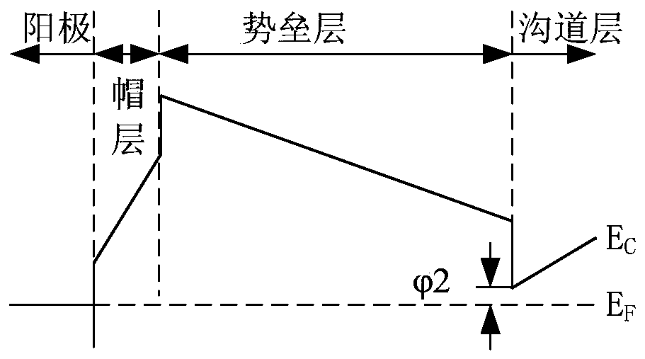
[0059] figure 1 It is a cross-sectional view of the gallium nitride diode provided by the first embodiment of the present invention when the conduction channel is closed. like figure 1 As shown, the gallium nitride diode includes: a substrate 11, a first channel layer 131 located on the substrate 11, a first barrier layer 141 located on the first channel layer 131, the first barrier layer 141 and A first two-dimensional electron gas 151 is formed at the interface of the first channel layer 131, the cap layer structure 16 located on the first barrier layer 141 is located on the first barrier layer 141 on the side of the cap layer structure 16 and / or Or extend to the cathode 17 within the first barrier layer 141, a gap is provided between the cap layer structure 16 and the cathode 17, located on the first barrier layer 141 on the other side of the cap layer structure 16 and / or extend to the first an anode within the barrier layer 141 , and the anode covers the upper surface of...

Embodiment 2

[0093] Figure 6 It is a cross-sectional view when the conduction channel of the gallium nitride diode provided by the second embodiment of the present invention is closed. like Figure 6 As shown, different from the GaN diode provided in Embodiment 1 of the present invention, in the GaN diode provided in Embodiment 2 of the present invention, the surface area of ​​the first barrier layer 141 in contact with the cathode 17 and the first anode 181 Impurities are respectively doped to form doped regions 19 .

[0094] In this embodiment, the impurities may be silicon ions.

[0095] The first barrier layer doped with impurities forms an n-type heavily doped region. Afterwards, when the metal electrode is evaporated in this heavily doped region, due to the high doping concentration of the first barrier layer, the metal electrode and the first barrier layer The barrier width of the first barrier layer is relatively low, and the probability of electron tunneling is high. Therefore...

Embodiment 3

[0101] Figure 9 It is a cross-sectional view when the conduction channel of the gallium nitride diode provided by the third embodiment of the present invention is closed. like Figure 9 As shown, different from the gallium nitride diode provided in Embodiment 1 of the present invention, the gallium nitride diode further includes: a first barrier layer located under the cap layer structure 16 and between the cap layer structure 16 and the cathode 17 The second channel layer 132 on 141, the second barrier layer 142 on the second channel layer 132 between the cap structure 16 and the second channel layer 132 and between the cap structure 16 and the cathode 17, A second two-dimensional electron gas 152 is formed at the interface between the second barrier layer 142 and the second channel layer 132 .

[0102] The second barrier layer 142 and the second channel layer 132 form a heterojunction structure, and a second two-dimensional electron gas 152 is formed at the interface betw...


PUM

PropertyMeasurementUnit
thicknessaaaaaaaaaa

Abstract

The present invention discloses a gallium nitride diode and a manufacturing method thereof. The gallium nitride diode comprises a substrate; a first channel layer disposed above the substratel a first barrier layer disposed on the first channel layer, a first two-dimensional electron gas being formed between the first barrier layer and the first channel layer; a cap layer structure disposed on the first barrier layer; a cathode disposed on the first barrier layer at one side of the cap layer structure and / or extending into the first barrier layer, a gap being arranged between the cap layer structure and the cathode; and anodes disposed at the first barrier layer at the other side of the cap layer structure and / or extending into the first barrier layer, the anodes covering to an upper surface of the cap layer structure. The gallium nitride diode provided by the present invention has characteristics of being low in threshold voltage and on resistance, high in positive breakover current and negative withstanding voltage, and low in negative electric leakage.

Description

technical field [0001] The invention relates to the technical field of semiconductors, in particular to a gallium nitride diode and a manufacturing method thereof. Background technique [0002] As the basic building block of electronic power, diodes are an indispensable part of voltage regulators, rectifiers and inverters. With the development of modern power electronics, diodes have put forward higher requirements on the performance of high breakdown voltage, low power consumption and low leakage. [0003] The semiconductor material gallium nitride (GaN) has the characteristics of large band gap, high thermal conductivity, and strong breakdown field, which makes GaN devices have the advantages of low on-resistance and high operating frequency, which can meet the requirements of modern power electronics development. requirements. [0004] At present, diodes based on GaN materials have made great progress. Most of the existing GaN Schottky diodes achieve rectification char...

Claims


Application Information

Patent Timeline
Patent Type & Authority Patents(China)
IPC IPC(8): H01L29/872H01L29/06H01L21/329
CPCH01L29/0611H01L29/0638H01L29/66143H01L29/872
Inventor 裴轶邓光敏张乃千
Owner GPOWER SEMICON
Why Eureka
Try Eureka