A kind of photosensitive diode and preparation method thereof

A photodiode and photosensitive technology, applied in the field of optoelectronics, can solve the problems of low narrow-wave spectral response performance, large wavelength range, poor stability, etc., and achieve the effect of overcoming low narrow-wave spectral response performance, narrow spectral absorption range, and strong absorption intensity.

Active Publication Date: 2019-04-02
TSINGHUA UNIV
View PDF3 Cites 0 Cited by
  • Summary
  • Abstract
  • Description
  • Claims
  • Application Information

AI Technical Summary

Problems solved by technology

[0005] Therefore, the technical problem to be solved in the present invention is to overcome the defects of the narrow spectral response photodiode in the prior art that the spectral response wavelength range is relatively large and the narrow spectral response performance is low, thereby providing a photosensitive diode with high performance narrow spectral response and its preparation method
[0006] Another technical problem to be solved by the present invention is to overcome the defect of poor stability of the narrow spectral response photodiode in the prior art, thereby providing a highly stable narrow spectral response photodiode and its preparation method

Method used


Image

  • A kind of photosensitive diode and preparation method thereof
  • A kind of photosensitive diode and preparation method thereof
  • A kind of photosensitive diode and preparation method thereof

Examples


Embodiment 1

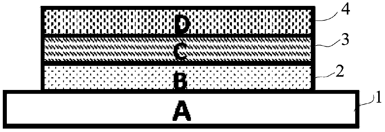
[0047] This embodiment provides a photosensitive diode, such as figure 1 As shown, it includes: a substrate 1, a first electrode layer 2, a single photosensitive absorption material layer 3 and a second electrode layer 4; the first electrode layer 2 is arranged on the substrate 1; the single photosensitive absorption material layer 3 It is arranged on the first electrode layer 2, and the half-width peak width of the absorption spectrum of the single photosensitive absorption material layer 3 is lower than 80 nm; the second electrode layer 4 is arranged on the single photosensitive absorption material layer 3, and The first electrode layer (2) is electrically connected and matches the work function of the single photosensitive absorption material layer 3 .

[0048] Specifically, the substrate 1 can be a colored or colorless transparent substrate, which can be rigid or flexible. When the substrate 1 is a colored transparent substrate, it can play the role of a filter. When the s...

Embodiment 2

[0066] This embodiment provides a method for preparing the photodiode described in Embodiment 1, such as Figure 11 shown, including the following steps:

[0067] S1. Forming the first electrode layer of the photodiode on the substrate.

[0068] S2. Forming a single photosensitive absorption material layer and a second electrode layer sequentially on the first electrode layer.

[0069] S3. Electrically connecting the first electrode layer and the second electrode layer.

[0070] Specifically, the preparation process of the above-mentioned first electrode layer, single photosensitive absorbing material layer and second electrode layer may be one or a combination of sputtering, spin coating, evaporation, and solution method to grow single crystals. The connection between the first electrode layer and the second electrode layer can be realized by forming the pins of the first electrode layer of the photodiode and the pins of the second electrode layer on the substrate, and ele...


PUM


Abstract

The invention provides a photosensitive diode and a preparation method thereof, wherein the photosensitive diode includes a substrate, a first electrode layer, a single photosensitive absorption material layer and a second electrode layer; the first electrode layer is arranged on the substrate; the single photosensitive absorption material layer is arranged On the first electrode layer, and the half-width peak width of the absorption spectrum of the single photosensitive absorption material layer is lower than 80nm; the second electrode layer is arranged on the single photosensitive absorption material layer, and is electrically connected to the first electrode layer, and It matches the work function of a single photosensitive absorbing material layer. Thus, a Schottky barrier structure is formed at the interface between the second electrode layer and the single photosensitive absorption material layer, which only generates photoresponse to specific light in the spectral absorption range, so the photosensitive diode of the present invention only adopts a single photosensitive absorption The material can realize the rectification characteristics of the photodiode, and there is no need to add an additional filter to filter out stray light to improve the narrow-spectrum response performance of the photodiode, which saves space.

Description

technical field [0001] The invention relates to the field of optoelectronics, in particular to a photosensitive diode and a preparation method thereof. Background technique [0002] Photodiode is a semiconductor device that converts optical signals into electrical signals. It has unidirectional conductivity, so a reverse voltage needs to be applied when working. When there is no light, the reverse current is very small (generally less than 0.1 microampere), which is called dark current. When there is light, the photons carrying energy enter the PN junction, and transfer the energy to the bound electrons on the covalent bond, so that some electrons break free from the covalent bond, thereby generating electron-hole pairs, which are called photogenerated carriers. . They participate in the drift movement under the action of reverse voltage, which makes the reverse current significantly larger. The greater the intensity of light, the greater the reverse current, this charact...

Claims


Application Information

Patent Timeline
Patent Type & Authority Patents(China)
IPC IPC(8): H01L51/42H01L51/46H01L51/48
CPCH10K85/657H10K30/451Y02E10/549Y02P70/50
Inventor 董桂芳李文海李东邱勇
Owner TSINGHUA UNIV
Why Eureka
Try Eureka