Lateral insulated gate bipolar transistor

Inactive Publication Date: 2011-12-01
DENSO CORP
View PDF3 Cites 20 Cited by
  • Summary
  • Abstract
  • Description
  • Claims
  • Application Information

AI Technical Summary

Benefits of technology

[0017]Also in the lateral IGBT according to the fourth aspect, the on-voltage can be reduced, th

Problems solved by technology

Because a current density in a lateral IGBT at operation is much higher than a current density in

Method used


Image

  • Lateral insulated gate bipolar transistor
  • Lateral insulated gate bipolar transistor
  • Lateral insulated gate bipolar transistor

Examples


first embodiment

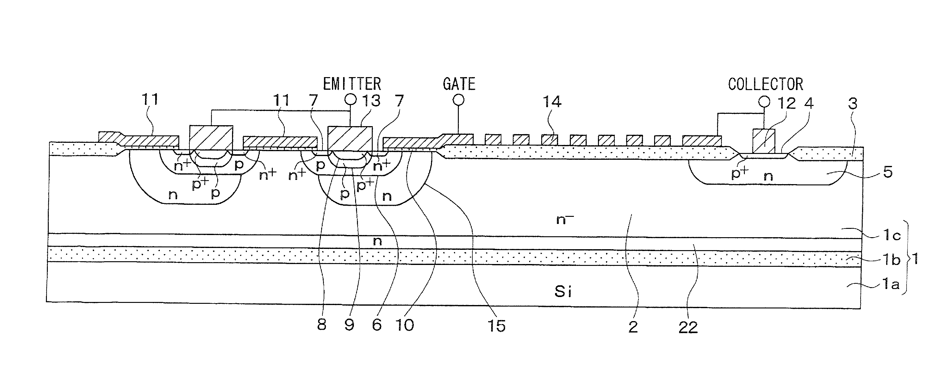
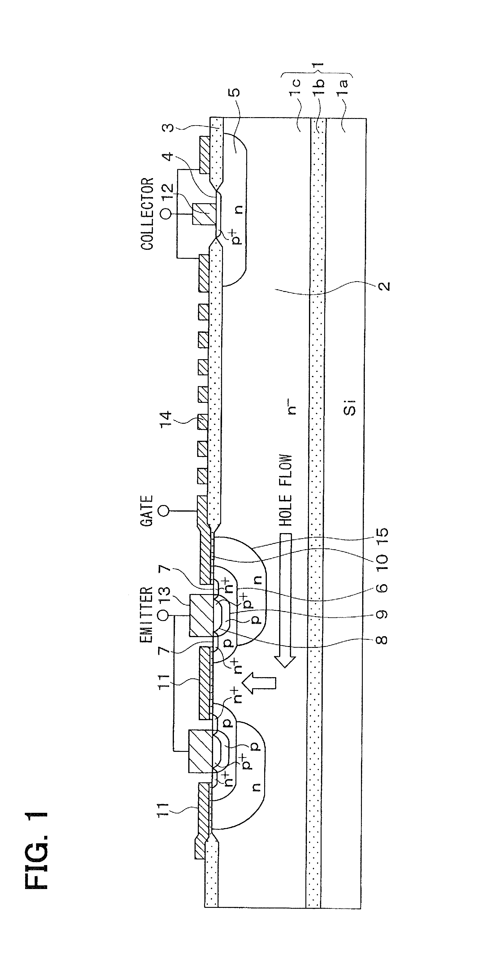
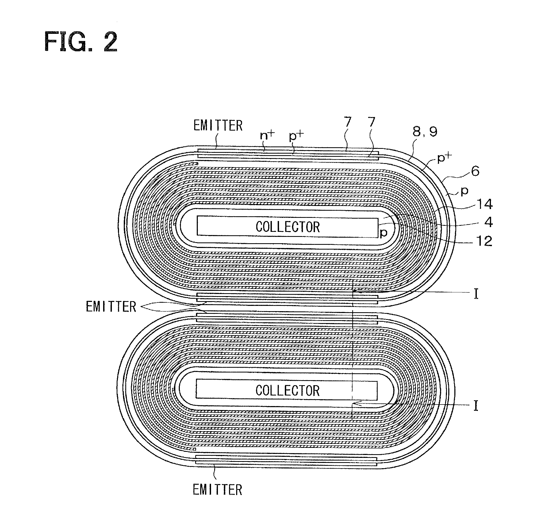
[0047]A lateral IGBT according to a first embodiment of the present invention will be described with reference to FIG. 1 and FIG. 2. FIG. 1 is a cross-sectional view of a semiconductor device including the lateral IGBT according to the present embodiment. FIG. 1 corresponds to a cross-sectional view of the semiconductor device taken along line I-I in FIG. 2.

[0048]As shown in FIG. 1, in the present embodiment, the lateral IGBT is formed using a silicon-on-insulator (SOI) substrate 1. The SOI substrate 1 includes a support substrate 1a made of, for example, silicon, a buried oxide layer 1b disposed on the support substrate 1a, and an active layer 1c made of silicon and disposed on the buried oxide layer 1b. The active layer 1c operates as an n− type drift layer 2. Each component in the lateral IGBT is disposed at a surface portion of the n− type drift layer 2.

[0049]In the SOI substrate 1, the buried oxide layer 1b can have any thickness and the active layer 1c (the n− type drift layer...

second embodiment

[0073]A semiconductor device including a lateral IGBT according to a second embodiment of the present invention will be described with reference to FIG. 7.

[0074]As shown in FIG. 7, in the present embodiment, the n type barrier layer 15 is disposed also between adjacent emitters, that is, between adjacent channel p well layers 6. If the n type barrier layer 15 has an impurity concentration same as the first embodiment, the structure of the lateral IGBT is similar to a structure of a lateral IGBT according to the prior art and the turning-off time increases. Thus, in the present embodiment, an n type impurity peak concentration of the n type barrier layer 15 is set to be within a range from 2×1015 cm−3 to 1.5×1016 cm−3.

[0075]FIG. 8 is a graph showing a relationship between the n type impurity peak concentration of the n type barrier layer 15 and an on-voltage (Von) of the lateral IGBT and a relationship between the impurity concentration of the n type barrier layer 15 and a switching ...

third embodiment

Modifications of Third Embodiment

[0085]The n type barrier layer 15 may be provided in the lateral IGBT according to the third embodiment.

[0086]For example, as shown in FIG. 12, the n type barrier layer 15 may be disposed to a depth deeper than the channel p well layer 6 so as to cover the channel p well layer 6, that is, to couple adjacent trenches 16. As shown in FIG. 13, the n type barrier layer 15 may also be formed so as to extend across the trench 16 located between adjacent cells, that is, to cover the two channel p well layers 6 in the adjacent cells.

[0087]By combining the trench 16 and the n type barrier layer 15, the n type barrier layer 15 can function as a barrier of holes, the carrier concentration of the n− type drift layer 2 in the vicinity of the emitter can be further increased, and the on-voltage can be further reduced. Furthermore, because a parasitic npn transistor provided in the vicinity of the emitter does not operate, an increase in the switching time can be r...


PUM


Abstract

A lateral insulated gate bipolar transistor includes a semiconductor substrate including a drift layer, a collector region, a channel layer, an emitter region, a gate insulating layer, a gate electrode, a collector electrode, an emitter electrode, and a barrier layer. The barrier layer is disposed along either side of the collector region and is located to a depth deeper than a bottom of the channel layer. The barrier layer has an impurity concentration that is higher than an impurity concentration of the drift layer. The barrier layer has a first end close to the collector region and a second end far from the collector region. The first end is located between the channel layer and the collector region, and the second end is located on the bottom of the channel layer.

Description

CROSS REFERENCE TO RELATED APPLICATIONS[0001]The present application is based on and claims priority to Japanese Patent Applications No. 2010-120545 filed on May 26, 2010, and No. 2010-219357 filed on Sep. 29, 2010, the contents of which are incorporated in their entirety herein by reference.BACKGROUND OF THE INVENTION[0002]1. Field of the Invention[0003]The present invention relates to a lateral insulated gate bipolar transistor (lateral IGBT).[0004]2. Description of the Related Art[0005]Japanese Patent No. 3,522,983 (corresponding to U.S. Pat. No. 5,731,603 and referred to as a patent document 1 hereafter) discloses a lateral IGBT in which the number of channels is increased to reduce an on-voltage. The patent document 1 also discloses that preventing operation of a parasitic thyristor is important to improve a latch-up immunity. This is because a current density in silicon in a lateral IGBT is much higher than a current density in silicon in a vertical IGBT. In a vertical IGBT, b...

Claims


Application Information

Patent Timeline
IPC IPC(8): H01L29/739
CPCH01L29/0696H01L29/0834H01L29/7394H01L29/405H01L29/7393H01L29/1095
Inventor TAKAHASHI, SHIGEKITOKURA, NORIHITOSHIRAKI, SATOSHIASHIDA, YOUICHINAKAGAWA, AKIO
Owner DENSO CORP
Why Eureka
Try Eureka