Technique for manufacturing back of non-through insulated-gate bipolar transistor chip

A bipolar transistor, non-punch-through technology, used in semiconductor/solid-state device manufacturing, electrical components, circuits, etc., can solve the problems of weakening the conductance modulation effect, high on-voltage, and high on-resistance, so as to enhance the conductance modulation effect. , the effect of reducing the on-resistance and on-voltage, and increasing the number of holes

Active Publication Date: 2010-07-28
TSINGHUA UNIV
View PDF0 Cites 20 Cited by
  • Summary
  • Abstract
  • Description
  • Claims
  • Application Information

AI Technical Summary

Problems solved by technology

However, NPT IGBT also has its important disadvantages, that is, its turn-on voltage is relatively high
This is mainly because the aluminum metallization process has been completed on the front side of the silicon wafer, and the temperature after boron ion implantation on the back side of the silicon wafer is limited (generally not exceed

Method used


Image

  • Technique for manufacturing back of non-through insulated-gate bipolar transistor chip
  • Technique for manufacturing back of non-through insulated-gate bipolar transistor chip
  • Technique for manufacturing back of non-through insulated-gate bipolar transistor chip

Examples


Embodiment Construction

[0013] The present invention will be described in detail below in conjunction with the accompanying drawings and embodiments.

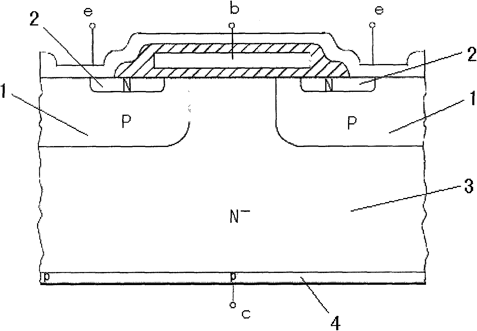
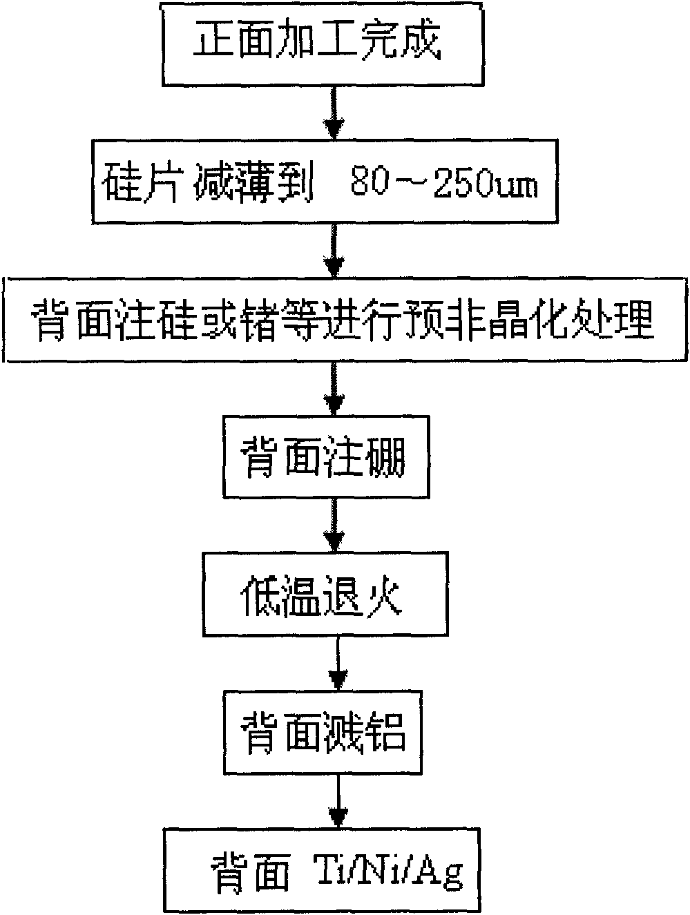
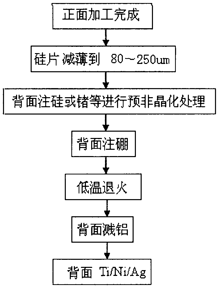
[0014] like figure 2 As shown, the present invention adopts the method of pre-amorphization treatment on the crystal back surface of the insulated gate bipolar transistor (IGBT) and low-temperature heat treatment to improve the boron ion activation of the crystal back of the non-punch-through insulated gate bipolar transistor (NPT IGBT). Rate. The steps are as follows:

[0015] 1) Complete the front-side process of the non-punch-through insulated gate bipolar transistor silicon wafer;

[0016] 2) Using grinding wheel grinding method, from the back of the silicon wafer of the non-punch-through insulated gate bipolar transistor, the silicon wafer is thinned to a thickness of 80-250um, and the necessary stress relief treatment is carried out;

[0017] 3) Implanting silicon ions, germanium ions or boron difluoride ions on the back of the silicon wafer...


PUM


Abstract

The invention relates to a technique for manufacturing the back of a non-through insulated-gate bipolar transistor chip, comprising the following steps of: (1) finishing a technique for processing the front of the non-through insulated-gate bipolar transistor chip; (2) grinding and thinning the back of a silicon chip, and removing stress; (3) injecting silicon ion, germanium ion or boron difluoride ion at the back of the silicon chip for amorphous pretreatment; (4) injecting boron ion at the back of the silicon chip; (5) carrying out furnace tube low temperature annealing; (6) adopting a sputtering or an evaporating method, generating an aluminium film at the back of the silicon chip, and carrying out alloy treatment; and (7) adopting the sputtering or the evaporating method, respectively preparing a titanium, a nickel and a silver metal layers at the back of the silicon chip. The back of the silicon chip is firstly injected with the silicon ion, the germanium ion or the boron difluoride ion for amorphous pretreatment and then injected with the boron ion for low-temperature annealing, so that the activation rate of injecting the boron impurity is improved, the conductive modulation effect for a drifting area can be enhanced, and the conducting resistance and conducting voltage are effectively reduced. The technique can be widely applied to a manufacturing technique of a semiconductor.

Description

technical field [0001] The invention relates to a semiconductor manufacturing process, in particular to a manufacturing process for the back surface of a non-piercing insulated gate bipolar transistor (NPT IGBT) crystal back collector boron ion activation rate . Background technique [0002] Insulated gate bipolar transistor (IGBT) is a semiconductor power device that integrates metal oxide semiconductor field effect transistor (MOSFET) and bipolar transistor (BJT) technology, and is widely used in high-power power electronics technology. As a voltage-controlled MOS / bipolar composite device, IGBT has the main advantages of bipolar junction power transistors and power metal oxide semiconductor field effect transistors (MOSFETs): high input impedance, low input drive power, and conduction Small resistance, large current capacity and fast switching speed. like figure 1 As shown, the working principle of a high-voltage N-channel enhancement type IGBT device is: when the volta...

Claims


Application Information

Patent Timeline
IPC IPC(8): H01L21/331
Inventor 刘志弘张伟崔杰许平
Owner TSINGHUA UNIV
Why Eureka
Try Eureka