Semiconductor element, semiconductor device, and electric power converter

a semiconductor and semiconductor technology, applied in the field of semiconductor devices, can solve the problems of reducing switching rate, not only recovery loss, but increasing stacking defects, etc., and achieve the effects of reducing the number of crystal imperfections, reducing the number of conductor losses, and high turn-on voltag

Active Publication Date: 2012-06-07
PANASONIC INTELLECTUAL PROPERTY MANAGEMENT CO LTD
View PDF0 Cites 22 Cited by
  • Summary
  • Abstract
  • Description
  • Claims
  • Application Information

AI Technical Summary

Benefits of technology

[0061]According to the present invention, the diode current is made to flow through a channel, not a body diode formed by a pn junction, and therefore, the turn-on voltage becomes lower than that of the body diode and the conduction loss can be reduced. This is even more effective for a wide bandgap semiconductor such as a silicon carbide semiconductor, in particular, because the body diode of such a semiconductor will have a high turn-on voltage. In addition, by lowering as much as possible the turn-on voltage of the diode at room temperature (25° C.), at which current flows through the channel, the voltage directly applied to the pn junction of the silicon carbide semiconductor can be kept less than the turn-on voltage (of 2.7 V) of the body diode. As a result, the increase in the number of crystal imperfections that would otherwise be caused by supplying a forward current to the pn junction of a silicon carbide semiconductor can be avoided. On top of that, since the diode performs a unipolar operation, not the bipolar operation, the reverse recovery current can be reduced. As a result, the loss involved by the reverse recovery current and the switching loss can both be reduced, and the diode can be switched at increased rates. What is more, with this element, the power converter no longer needs to have a freewheeling diode element, and therefore, the number of components required can be reduced. In other words, according to the present invention, a single element can operate as either an MISFET or a diode according to the voltage applied to an electrode of that element. Consequently, the circuit cost can be cut down.

Problems solved by technology

Somebody reported that if a forward current is supplied to the pn junction of SiC, stacking defects will increase due to basal plane dislocations, which is a problem unique to SiC.
Such a problem will arise when a SiC-FET is used as a switching element for a power converter for driving and controlling a load such as a motor.
And that reverse recovery current causes not only recovery loss but also a decrease in switching rate as well.
Since SiC is a wide bandgap semiconductor, the body diode 180 has a relatively high turn-on voltage Vf of around 3 V (e.g., approximately 2.7 V) at room temperature and would cause a lot of loss.
Also, as mentioned above, if the body diode 180 is used as a freewheeling diode, the degree of crystallinity of the semiconductor element 1100 will decrease and its reliability will also decline eventually, which is a problem.
Also, if a forward current is continuously supplied to the pn junction of SiC, crystal imperfections of SiC will increase so much as to cause even more loss, which is a problem unique to SiC.
When the body diode 180 turns OFF, a reverse recovery current flows, thus causing some recovery loss.
As a result, as there is a period in which the reverse recovery current flows, it becomes very difficult to switch the semiconductor element 1100 at high rates.
In addition, since the switching loss increases, it becomes difficult to increase the switching frequency, too.
However, as indicated by the arrow 95 in FIG. 18, the reverse recovery current is superposed on the current flowing through the high-side MISFET H, thus causing an increase in switching loss, a breakdown of the element due to overcurrent, and a lot of noise.
As indicated by these curves (a) and (b), a pn junction diode has a period in which a reverse recovery current is generated, thus deteriorating the performance of the inverter circuit 1000 (e.g., interfering with the high-rate switching and increasing the switching loss).
However, SiC-SBD is expensive, which is a problem.
On top of that, if the number of components to use to make the inverter circuit 1000 is increased to cope with the return current, then the circuit cost will increase as well.

Method used


Image

  • Semiconductor element, semiconductor device, and electric power converter
  • Semiconductor element, semiconductor device, and electric power converter
  • Semiconductor element, semiconductor device, and electric power converter

Examples


embodiment 1

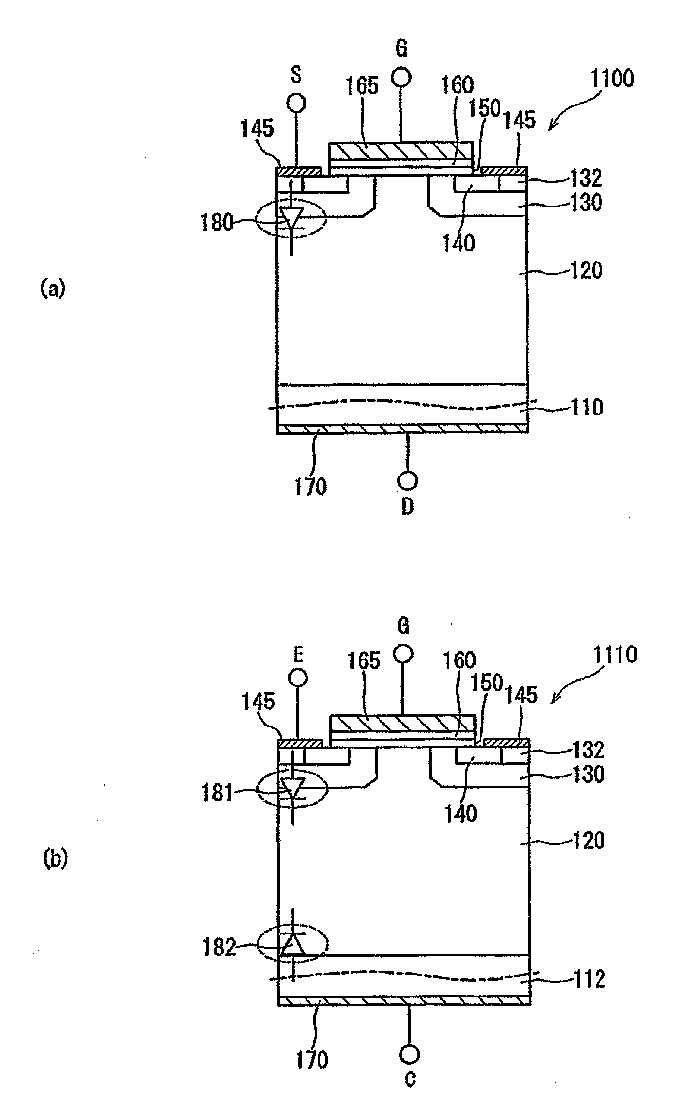
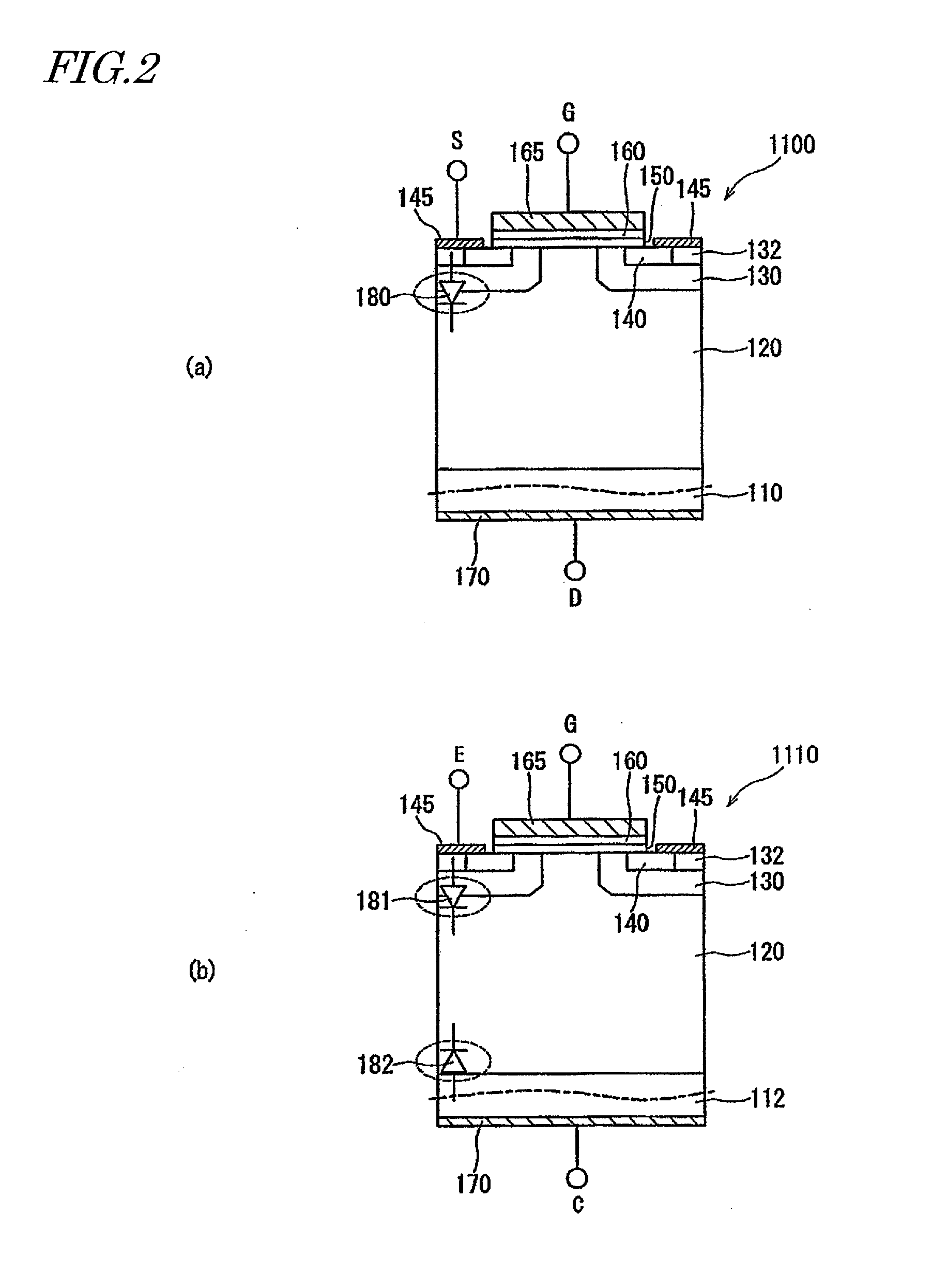
[0125]a Semiconductor Element 100 as a Preferred embodiment of the present invention will now be described with reference to FIGS. 5(a) and 5(b). FIG. 5(a) is a cross-sectional view schematically illustrating the structure of the semiconductor element100 of this preferred embodiment. On the other hand, FIG. 5(b) illustrates the semiconductor element 100 of this preferred embodiment by a circuit symbol. Specifically, the diode symbol shown in FIG. 5(b) represents a diode that makes a current flow through the channel region of the semiconductor element 100. Also, in FIG. 5(b), G, S and D denote a gate electrode, a source electrode and a drain electrode, respectively.

[0126]In this description, the potential of the drain electrode D with respect to the potential of the source electrode S will be identified herein by Vds. The potential of the gate electrode G with respect to the potential of the source electrode S will be identified herein by Vgs. The direction of a current flowing from ...

embodiment 2

[0232]Hereinafter, a second preferred embodiment of a semiconductor element according to the present invention will be described.

[0233]The first preferred embodiment of the present invention described above is a “vertical” semiconductor element, of which the drain electrode is arranged on the back surface of the substrate. On the other hand, this second preferred embodiment of the present invention is a “lateral” semiconductor element, of which the source and drain electrodes are arranged on the surface (principal surface) of the semiconductor layer. As what has already been described about the operation of the first preferred embodiment of the present invention is focused on the channel region, it makes almost no difference whether the drain electrode is arranged on the back surface or on the principal surface. That is why the foregoing description about the threshold voltage of the transistor and the turn-on voltage of the diode is applicable as it is to such a lateral transistor....

embodiment 3

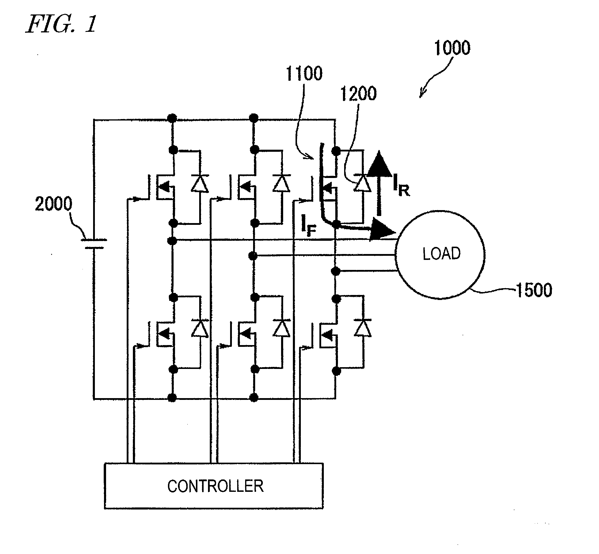
[0282]Hereinafter, a switching element 400 as a third preferred embodiment of the present invention will be described with reference to FIG. 41, which is a cross-sectional view schematically illustrating a configuration for the switching element 400 of this preferred embodiment.

[0283]Unlike the semiconductor element 100 of the second preferred embodiment described above, the drain region 75 is spaced apart from the stack of the epitaxial channel layer 50, the gate insulating film 60 and the gate electrode 65 in the switching element 400 of this preferred embodiment. That is to say, when viewed perpendicularly to the substrate 10, a portion of the region (i.e., the n− drift layer 20) between the source and drain regions 40 and 75 is not covered with the gate electrode 65. That portion not covered with the gate electrode 65 forms part of the n− drift layer 20 but may also be regarded as an extension of the drain region 75 and functions as an LDD (lightly doped drain) region. The LDD r...


PUM


Abstract

A semiconductor element 100 including an MISFET according to the present invention is characterized by having diode characteristics in a reverse direction through an epitaxial channel layer 50. The semiconductor element 100 includes a semiconductor layer 20 of a first conductivity type, a body region 30 of a second conductivity type, source and drain regions 40 and 75 of the first conductivity type, an epitaxial channel layer 50 in contact with the body region, source and drain electrodes 45 and 70, a gate insulating film 60, and a gate electrode 65. If the voltage applied to the gate electrode of the MISFET is smaller than a threshold voltage, the semiconductor element 100 functions as a diode in which current flows from the source electrode 45 to the drain electrode 70 through the epitaxial channel layer 50. The absolute value of the turn-on voltage of this diode is smaller than that of the turn-on voltage of a body diode that is formed of the body region and the first silicon carbide semiconductor layer.

Description

TECHNICAL FIELD[0001]The present invention relates to a semiconductor element and more particularly relates to a silicon carbide semiconductor element (as a power semiconductor device), which can be used in applications that require a high breakdown voltage and a large amount of current. The present invention also relates to a semiconductor device and power converter including such a silicon carbide semiconductor element.BACKGROUND ART[0002]Silicon carbide (SiC) is a high-hardness semiconductor material with a greater bandgap than silicon (Si), and has been used extensively in various types of semiconductor devices including power elements, hostile-environment elements, high temperature operating elements, and radio frequency elements. Among other things, the application of SiC to power elements such as semiconductor elements and rectifiers has attracted a lot of attention. This is because a power element that uses SiC can significantly reduce the power loss compared to a Si power e...

Claims


Application Information

Patent Timeline
Patent Type & Authority Applications(United States)
IPC IPC(8): G05F3/02H01L29/78
CPCH01L29/1608H01L29/66068H01L29/78Y02B70/1483H01L29/7838H02M7/5387H01L29/7828Y02B70/10
Inventor HASHIMOTO, KOICHIADACHI, KAZUHIROKUSUMOTO, OSAMUUCHIDA, MASAOKAZAMA, SHUN
Owner PANASONIC INTELLECTUAL PROPERTY MANAGEMENT CO LTD
Why Eureka
Try Eureka