

Semiconductor integrated circuit device
a technology of integrated circuits and semiconductors, applied in the direction of semiconductor devices, electrical equipment, transistors, etc., can solve the problems of difficult to efficiently improve the performance of transistors by using sti stress
- Summary
- Abstract
- Description
- Claims
- Application Information
AI Technical Summary
Problems solved by technology
Method used
Image

Examples
first embodiment
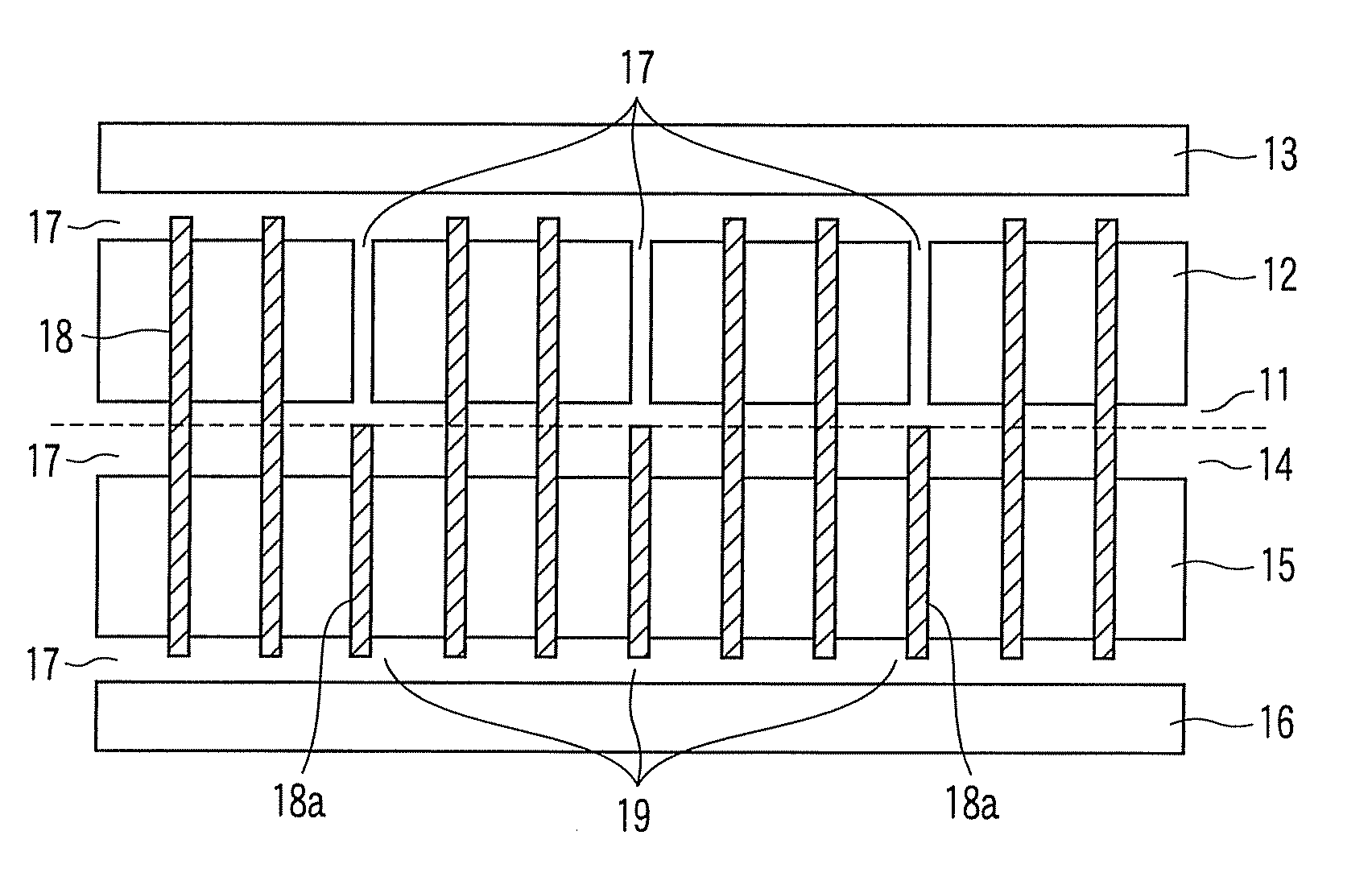
[0022]FIG. 1 shows a pattern layout according to a first embodiment. A semiconductor substrate has an N-well region 11 formed therein, in which the active regions 12 of P-channel transistors and an N-sub region 13 for making contact with an N-well lead-out electrode are formed. The semiconductor substrate further has a P-well region 14 formed therein, in which the active regions 15 of N-channel transistors and a P-sub region 16 for making contact with a P-well lead-out electrode are formed. STI regions 17 are respectively formed between the N-well region 11 and P-well region 14, between the active regions 12 and N-sub region 13, and between the active regions 15 and P-sub region 16. The active regions 12, N-sub region 13, active regions 15, and P-sub region 16 respectively have strip-like patterns, such that the active regions 12 are adjacent to the active regions 15, and the strip-like patterns extend parallel to each other as a whole.
[0023]Further, in this embodiment, STI regions ...
example of first embodiment
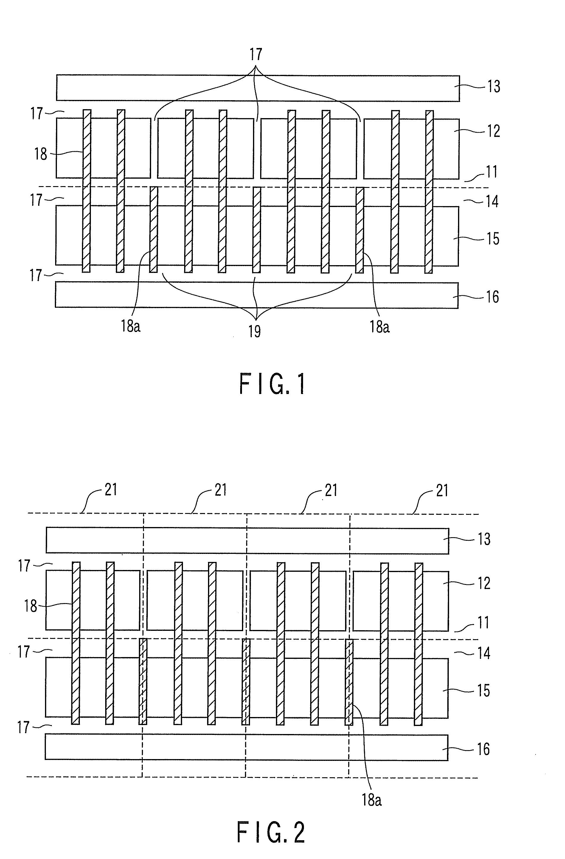
[0027]FIG. 2 is a view showing a gate array comprising a number of basic cells 21 arrayed in rows and columns. Each of the basic cells 21 is formed of the P-channel transistors in one unit portion of active regions 12 and the N-channel transistors in one unit portion of active regions 15 adjacent to each other in FIG. 1.
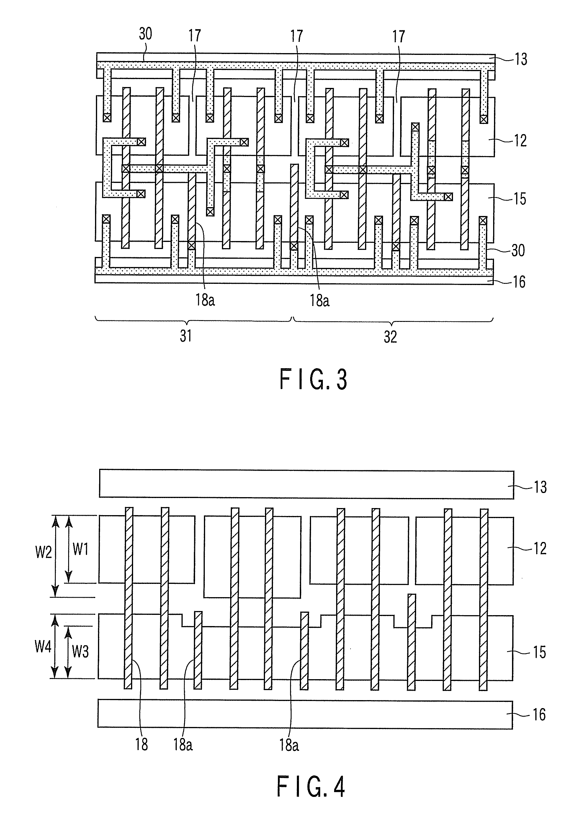
[0028]FIG. 3 is a view showing the pattern layout of a device where a two-input AND gate circuit 31 and a two-input OR gate circuit 32, which are of the CMOS type, are structured as an example of the gate array.
[0029]Each set of the two-input AND gate circuit 31 and two-input OR gate circuit 32 employs four P-channel transistors and four N-channel transistors. A P-sub region 16 is in contact with a metal interconnection line 30, which is in contact with dummy gate electrodes 18a for normally-off transistors in active regions 15, wherein a ground potential is applied to the dummy gate electrodes 18a. The active regions 15 are isolated from each other by gate isolation...
first modification
of First Embodiment
[0031]FIG. 4 is a view showing a first modification. In the pattern layout shown in FIG. 4, partly different transistor sizes are used in unit portions formed of the active regions 12 of P-channel transistors. Specifically, a part of the unit portions formed of the active regions 12 has a width W2 (the channel width of a P-channel transistor) greater than the width W1 of the other unit portions. On the other hand, a part of the unit portions formed of the active regions 15 of the N-channel transistors has a width W3 (the channel width of an N-channel transistor) smaller than the width W4 of the other unit portions. Further, the length (gate length) of gate electrodes 18a for normally-off transistors is set to be shorter in the active regions 15 of the N-channel transistors. In this case, it is possible to further improve the characteristic of the P-channel transistor having the greater channel width W2. Such a semiconductor integrated circuit device is suitable fo...
PUM
 Abstract
Description
Claims
Application Information