Pixel structure and liquid crystal display panel

Active Publication Date: 2007-11-22
AU OPTRONICS CORP
View PDF6 Cites 32 Cited by
  • Summary
  • Abstract
  • Description
  • Claims
  • Application Information

AI Technical Summary

Benefits of technology

[0012]Accordingly, an object of the present invention is to provide a pixel structure, suitable for eliminating the phenomeno

Problems solved by technology

However, the rising “environmental protection” awareness is against its power consumption and radiation disadvantage, and the limite

Method used


Image

  • Pixel structure and liquid crystal display panel
  • Pixel structure and liquid crystal display panel
  • Pixel structure and liquid crystal display panel

Examples


first embodiment

The First Embodiment

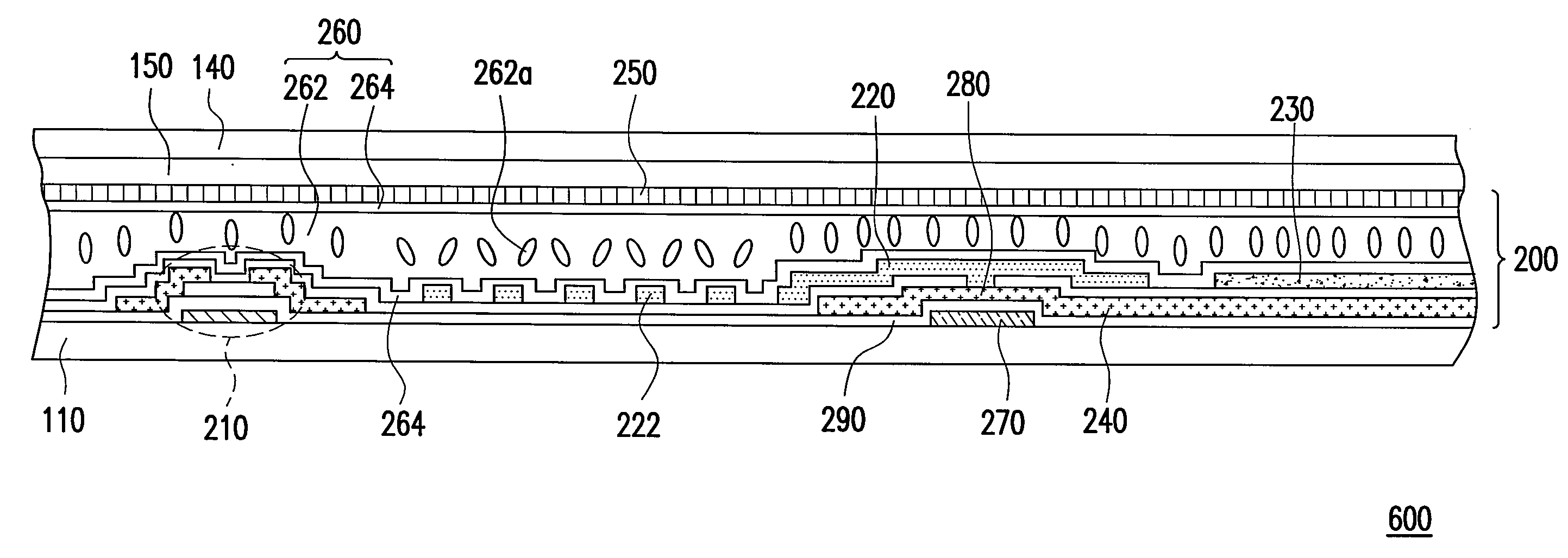
[0044]FIG. 2A is a partial schematic sectional view of an LCD panel according to the first embodiment of the present invention, and FIG. 2B is a top view of an active device array substrate according to the first embodiment of the present invention, wherein the schematic sectional view of the active device array substrate of FIG. 2A is taken along the section line B-B′ in FIG. 2B. Referring to FIGS. 2A and 2B, the LCD panel 600 of the present embodiment comprises a lower substrate 110, an upper substrate 140, a color filter array 150, and a plurality of pixel structures 200. A plurality of scan lines 120 and a plurality of data lines 130 are formed on the lower substrate 110. The color filter array 150 is disposed between the lower substrate 110 and the upper substrate 140. The pixel structures 200 are disposed between the color filter array 150 and the lower substrate 110. The detailed structure, arrangement position, connection relation, and material of various...

second embodiment

The Second Embodiment

[0056]FIG. 3A is a partial schematic sectional view of an LCD panel according to the second embodiment of the present invention, and FIG. 3B is a top view of an active device array substrate according to the second embodiment of the present invention, wherein the schematic sectional view of the active device array substrate of FIG. 3A is taken along the section line C-C′ in FIG. 3B. Referring to FIGS. 3A and 3B, the LCD panel 700 of the present embodiment is a variation of the LCD panel 600 of the first embodiment, and wherein the first pixel electrode 320 and the second pixel electrode 330 of the pixel structure 300 are respectively disposed on two opposite sides of the common line 270, and the coupling line 340 is not connected to the capacitor electrode 280.

[0057]As the advantages of the LCD panel 700 and the pixel structure 300 are substantially the same as those described in the first embodiment, the details will not be described herein again.

third embodiment

The Third Embodiment

[0058]FIG. 4A is a partial schematic sectional view of an LCD panel 800 according to the third embodiment of the present invention, and FIG. 4B is a top view of an active device array substrate according to the third embodiment of the present invention, wherein the schematic sectional view of the active device array substrate of FIG. 4A is taken along the section line D-D′ in FIG. 4B. Referring to FIGS. 4A and 4B, the LCD panel 800 of the present embodiment is a variation of the LCD panel 600 of the first embodiment, and wherein the second pixel electrode 430 of the pixel structure 400 comprises a first sub-pixel electrode 430a and a second sub-pixel electrode 430b. And the first sub-pixel electrode 430a and the second sub-pixel electrode 430b are disposed respectively on two opposite sides of the first pixel electrode 420.

[0059]As the advantages of the LCD panel 800 and the pixel structure 400 are substantially the same as those described in the first embodiment...


PUM


Abstract

A pixel structure including an active device, a first pixel electrode, a second pixel electrode, a coupling line, a common electrode, and a liquid crystal layer is provided. The first pixel electrode and the second pixel electrode have a plurality of sets of stripped electrode patterns extending along different directions, respectively, and the first pixel electrode is electrically insulated from the second pixel electrode. The coupling line is disposed under the first and the second pixel electrode and electrically insulated from the second pixel electrode. The first pixel electrode is electrically connected to the active device through the coupling line. The common electrode is disposed over the first and the second pixel electrode. The liquid crystal layer is disposed between the common electrode and the first and second pixel electrodes. Moreover, the liquid crystal layer has two polymer layers and a liquid crystal molecule layer disposed between the polymer layers.

Description

[0001]This application claims the benefit of Taiwan Patent Application Serial No. 95117813, filed on May 19, 2006. All disclosure of the Taiwan application is incorporated herein by reference.BACKGROUND OF THE INVENTION[0002]1. Field of Invention[0003]The present invention relates to a pixel structure. More particularly, the present invention relates to a pixel structure using polymer-stabilized alignment.[0004]2. Description of Related Art[0005]In response to the increasing demand of displays, the industry put efforts in the development of the display. Among the displays, the cathode ray tube (CRT) has occupied the display market for many years, due to its high display quality and mature technology. However, the rising “environmental protection” awareness is against its power consumption and radiation disadvantage, and the limited flattening capability is against the market demands, and thus the cathode ray tube (CRT) cannot meet the market demands gradually. Therefore, the thin fi...

Claims


Application Information

Patent Timeline
IPC IPC(8): G02F1/1337
CPCG02F2001/134345G02F1/134309G02F1/134345
Inventor HUANG, SHU-ISUN, WEI-CHIEHPENG, CHIH-YUCHEN, YA-CHIEHLAI, CHAI-LING
Owner AU OPTRONICS CORP
Why Eureka
Try Eureka