Wafer level package and method of fabricating the same

a technology of wafers and packages, applied in the field of wafer level packages, can solve the problems of increasing the number of defective products, increasing the manufacturing cost, etc., and achieve the effects of reducing the overall package thickness, reducing manufacturing costs, and improving reliability

Inactive Publication Date: 2007-11-22
SAMSUNG ELECTRONICS CO LTD
View PDF6 Cites 73 Cited by
  • Summary
  • Abstract
  • Description
  • Claims
  • Application Information

AI Technical Summary

Benefits of technology

[0019]Embodiments of the present invention provide a wafer level package with reduced fabricatio...

Problems solved by technology

However, according to conventional art, in order to construct the via hole 11 and an interconnection structure penetrating the via ho...

Method used


Image

  • Wafer level package and method of fabricating the same
  • Wafer level package and method of fabricating the same
  • Wafer level package and method of fabricating the same

Examples


Embodiment Construction

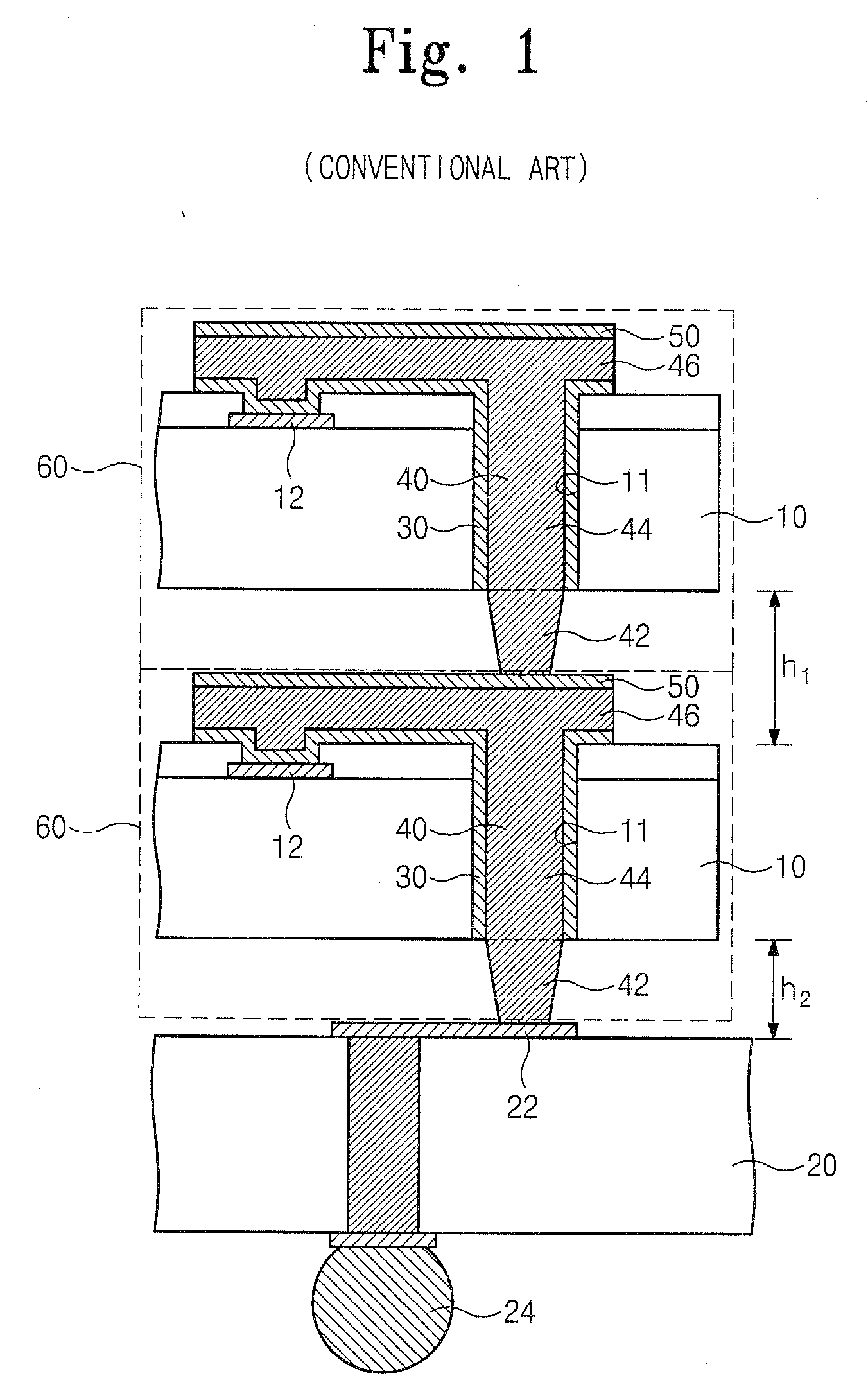
[0025]The present invention will now be described more fully hereinafter with reference to the accompanying drawings, in which preferred embodiments of the invention are shown. This invention, however, may be embodied in many different forms and should not be construed as limited to the embodiments set forth herein. Rather, these embodiments are provided so that this disclosure will be thorough and complete, and will fully convey the scope of the invention to those skilled in the art. In the drawings, the thicknesses of layers and regions are exaggerated for clarity. It will also be understood that when a layer is referred to as being “on” another layer or substrate, it can be directly on the other layer or substrate, or intervening layers may also be present. Like reference numbers refer to like elements throughout.

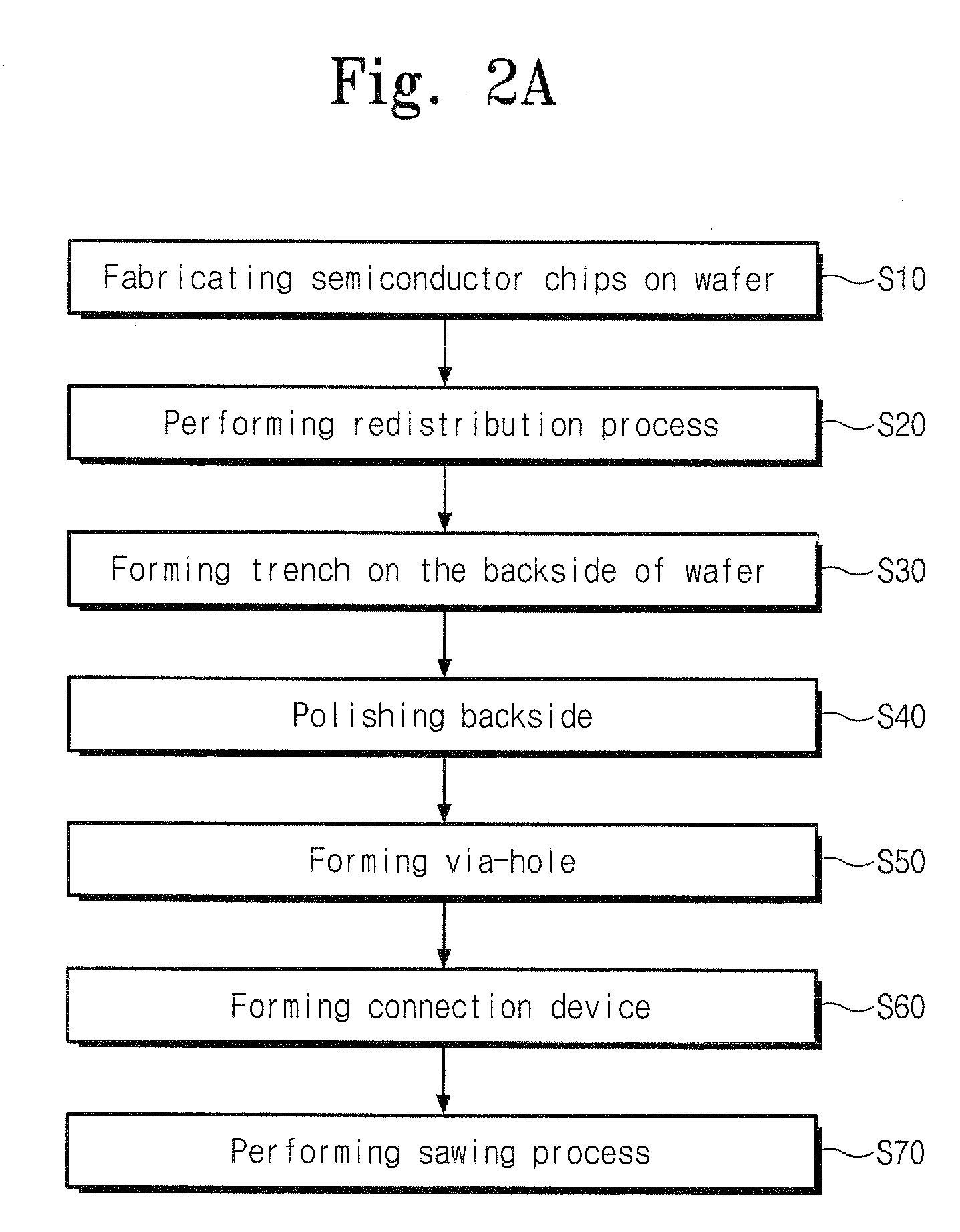
[0026]FIG. 2A is a process flow chart of a method of fabricating a wafer level package according to exemplary embodiments of the present invention. FIGS. 3A to 7A, FIG. ...


PUM


Abstract

Wafer level packages and methods of fabricating the same are provided. In one embodiment, one of the methods comprises forming semiconductor chips having a connection pad on a wafer, patterning a bottom surface of the wafer to form a trench under the connection pad, patterning a bottom surface of the trench to form a via hole exposing the bottom surface of the connection pad, and forming a connecting device connected to the connection pad through the via hole. The invention provides a wafer level package having reduced thickness, lower fabrication costs, and increased reliability compared to conventional packages.

Description

CROSS-REFERENCE TO RELATED APPLICATIONS[0001]This U.S. non-provisional patent application claims priority under 35 U.S.C. § 119 to Korean Patent Application No. 2006-45802, filed on May 22, 2006, the entire contents of which are hereby incorporated by reference.BACKGROUND[0002]1. Technical Field[0003]The present invention relates to a semiconductor package and a method of fabricating the same. More specifically, the present invention is directed to a wafer level package and a method of fabricating the same.[0004]2. Background of the Related Art[0005]Generally, semiconductor manufacturing can be divided into two kinds of processes. The two kinds of processes are a front-end process to manufacture IC chips on a wafer by means of processes such as photolithography / deposition / etch, and a back-end process involving assembling and packaging each of the IC chips. Four significant functions of the packaging process are as follows:[0006]1. Protection of the IC chips from the environment and ...

Claims


Application Information

Patent Timeline
IPC IPC(8): H01L21/00
CPCH01L21/76898H01L25/50H01L2924/0002H01L2224/94H01L2224/13025H01L2225/06513H01L2225/06541H01L2225/06555H01L2225/06586H01L2924/01029H01L2924/01038H01L2924/01079H01L2924/01093H01L2924/01006H01L2924/01024H01L2924/01033H01L2924/01047H01L2924/01074H01L25/0657H01L29/0657H01L2224/0401H01L2224/05548H01L2224/05567H01L2224/0557H01L2224/06181H01L2224/11H01L2224/05552H01L23/12
Inventor CHUNG, HYUN-SOOLEE, IN-YOUNGHWANG, SON-KWANLEE, DONG-HOHWANG, SEONG-DEOK
Owner SAMSUNG ELECTRONICS CO LTD
Why Eureka
Try Eureka