Antenna structure and method of manufacturing antenna

Inactive Publication Date: 2007-11-29
LG ELECTRONICS INC
View PDF13 Cites 9 Cited by
  • Summary
  • Abstract
  • Description
  • Claims
  • Application Information

AI Technical Summary

Benefits of technology

[0023] According to the present invention so configured, the antenna pattern is formed on the inner surface of the case of the terminal device. Therefore, even though the antenna pattern is complex, an antenna structure can be easily implemented. Further, an influence of noise on the antenna structure can be reduced since the antenna pattern is spaced apart from a printed circuit board by a predetermined distance.

Problems solved by technology

As shown in FIG. 1, however, since an antenna pattern 3 is manufactured on a structure 1 through the injection molding, it was difficult to process or correct the resultant antenna.
Accordingly, in a case where a pattern should be corrected due to a change of an antenna characteristic, it is difficult to perform an active design change for tuning and the manufacturing costs are high.
Further, there are problems in that the injection molding causes an increase of a defective proportion and the mold costs are incurred because molds for the injection molding should be manufactured.
Therefore, there was a limitation in minimizing the size of a terminal device since an installation space should be secured.
In this case, however, there is another problem in that the antenna pattern 13 may be influenced by noise produced in the other components mounted on the printed circuit board 11 or may interfere with the other components.
Therefore, additional works are required and the associated costs are thus increased.

Method used


Image

  • Antenna structure and method of manufacturing antenna
  • Antenna structure and method of manufacturing antenna
  • Antenna structure and method of manufacturing antenna

Examples


Embodiment Construction

[0030] Hereinafter, an antenna structure and a method of manufacturing an antenna according a preferred embodiment of the present invention will be described in detail with reference to the accompanying drawings.

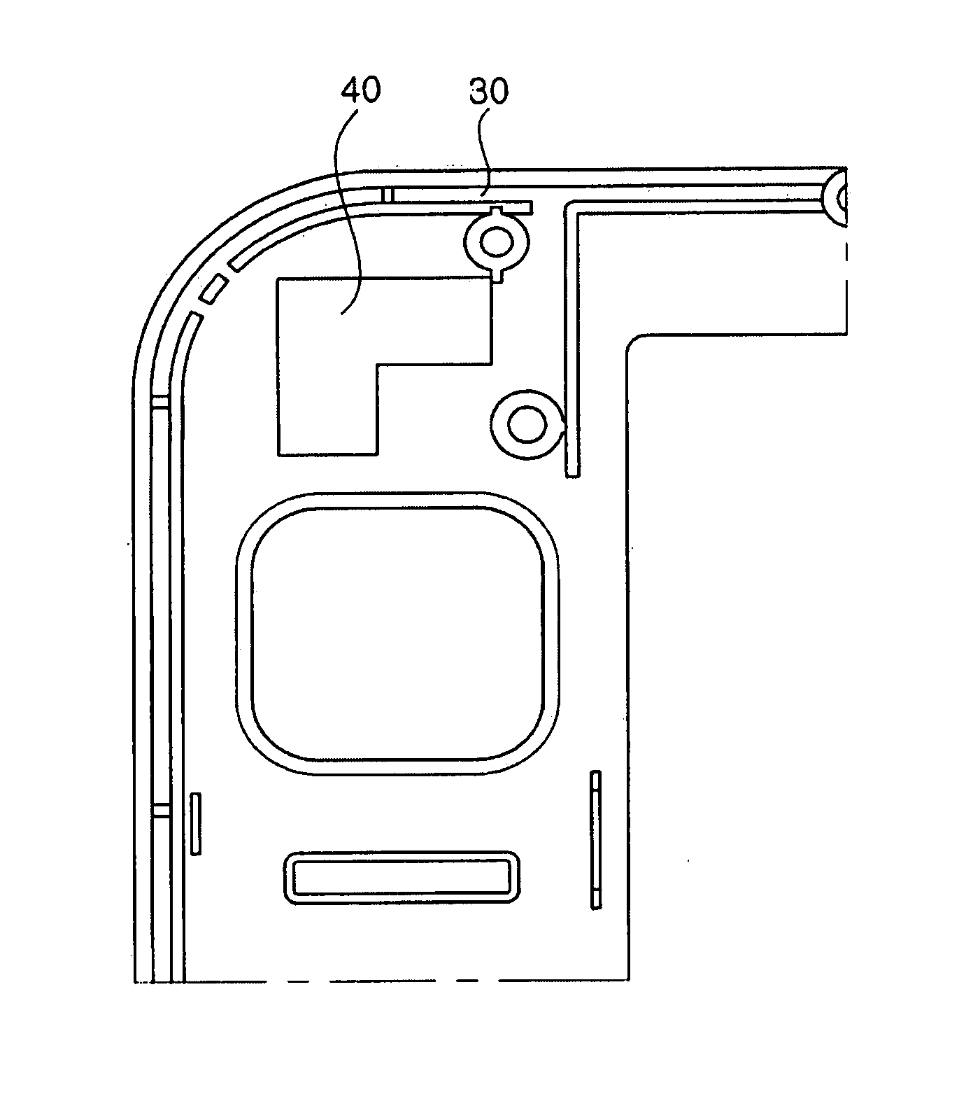
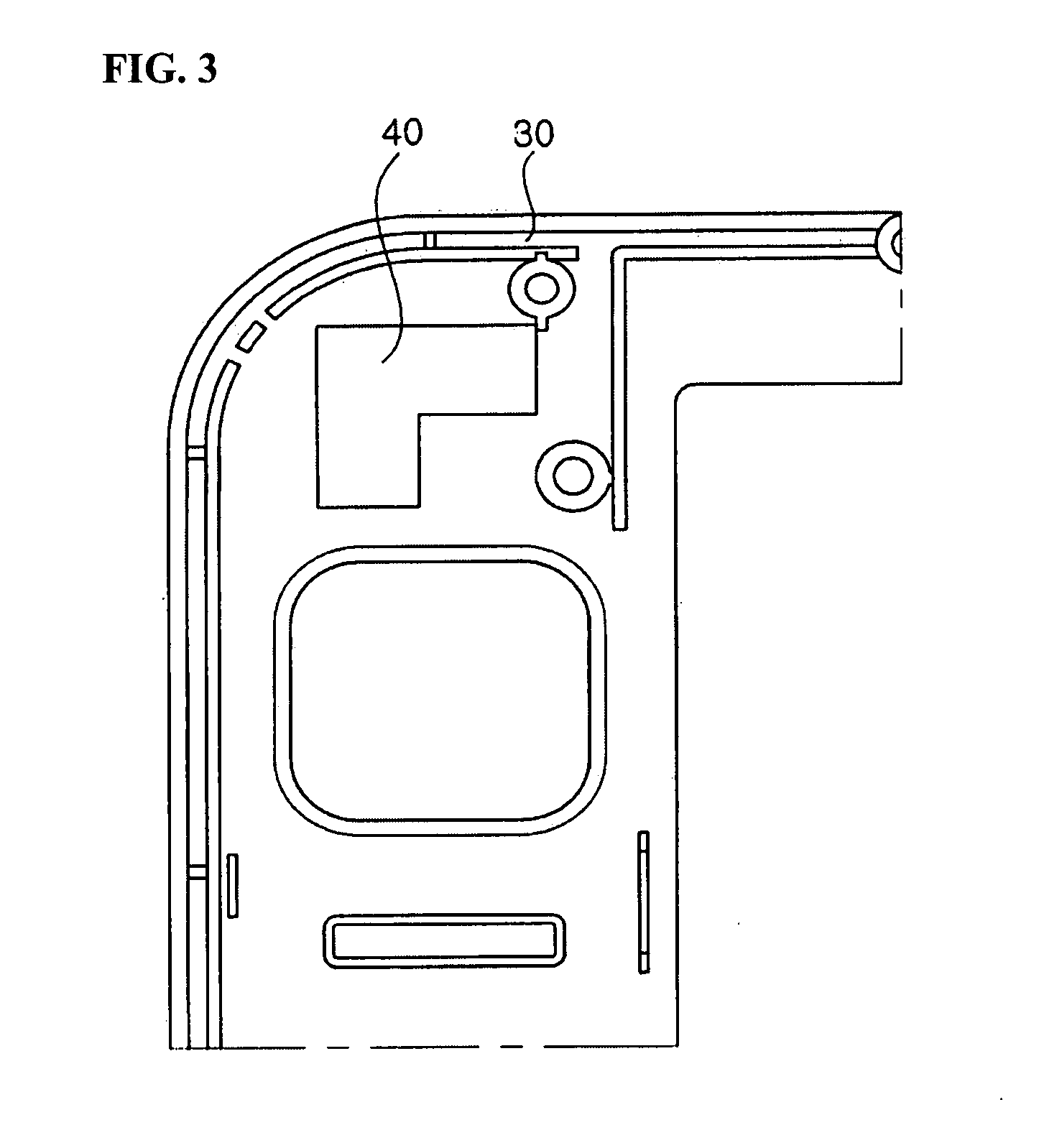
[0031]FIG. 3 is a view showing the configuration of an antenna structure according to a preferred embodiment of the present invention, and FIG. 4 is a view illustrating a process of forming the antenna structure of the present invention shown in FIG. 3 by printing an antenna pattern on an inner surface of a case of a terminal device.

[0032] Referring to FIGS. 3 and 4, it can be understood that an antenna pattern 40 is printed on an inner surface of a case 30 of a terminal device. The antenna pattern 40 has different shapes according to frequency characteristics of various wireless communication methods such as Bluetooth, WLAN, GSM or CDMA. Accordingly, the antenna pattern 40 should be formed into a pattern with an optimal antenna characteristic in consideration of the chara...


PUM


Abstract

The present invention relates to an antenna structure in which an antenna pattern is formed on an inner surface of a case of a terminal device, and a method of manufacturing an antenna. In the present invention, an optimal antenna pattern is shaped in accordance with a frequency characteristic of a terminal device and the antenna pattern is directly printed on an inner surface of the terminal device through a vacuum evaporation or sputtering method. At this time, a mask member having the same shape as that of the antenna pattern is further provided. Alternatively, a transfer paper with the antenna pattern printed thereon may be attached to the inner surface of the terminal device. Therefore, even a complex antenna pattern can be easily implemented in the terminal device. Further, an optimal antenna characteristic can be obtained since the antenna is spaced apart from a printed circuit board by a predetermined distance.

Description

BACKGROUND [0001] 1. Field of the Invention [0002] The present invention relates to an internal antenna, and more particularly, to an antenna structure in which an antenna pattern is formed on an inner surface of a case of a terminal device, and a method of manufacturing an antenna. [0003] 2. Description of the Related Art [0004] In general, an antenna for data transmission and reception is essential in order to perform a function such as Bluetooth corresponding to a typical local area wireless communication, a wireless local area network (WLAN), a global system for mobile communication (GSM) or code division multiple access (CDMA) in a terminal device such as cellular phone, PDA or PMP. The antenna should be able to provide an almost omnidirectional radiation pattern and a relative high gain and bandwidth. Further, in order to implement a multi-band and multi-mode operation, various bands should be able to be easily implemented. In this case, it is technically important to design a...

Claims


Application Information

Patent Timeline
IPC IPC(8): H01Q1/24
CPCH01Q1/38H01Q1/243H01Q1/20
Inventor HONG, BONG KUK
Owner LG ELECTRONICS INC
Why Eureka
Try Eureka