Semiconductor device

Inactive Publication Date: 2010-10-21
SEMICON ENERGY LAB CO LTD
View PDF9 Cites 0 Cited by
  • Summary
  • Abstract
  • Description
  • Claims
  • Application Information

AI Technical Summary

Benefits of technology

[0012]Thus, an embodiment of the present invention provides a semiconductor device having a circuit which can generate a demodulation signal (a demodulation signal generation circuit) without any problem also as to a modulation signal whose modulation factor is small (e.g., a signal whose modulation factor is 10%).
[0020]When the potential of a demodulation signal is inverted from HIGH to LOW, the potential of an output of the pulse detection circuit is inverted from LOW to HIGH. After that, the potential of the output of the pulse detection circuit remains at HIGH even when the potential of the demodulation signal is inverted from LOW to HIGH and then inverted from HIGH to LOW. When the potential of the demodulation signal returns to HIGH and does not change to LOW for a certain period of time, the potential of the output of the pulse detection circuit returns to LOW. When the potential of a signal of the pulse detection circuit is inverted to HIGH, the voltage level of an output signal of a bias circuit is changed. This prevents time change of demodulation signals in pulse width in such a manner that the voltage level of the first bias circuit and the voltage level of the second bias circuit approximate to each other. It is preferable that the voltage levels of the first bias circuit and the second bias circuit originally approximate to each other; however, demodulation signals have influence of noise when the voltage levels approximate to each other from the beginning. Therefore, the voltage levels approximate to each other in the middle of change in output voltage levels of output signals of the bias circuits. In an embodiment of the present invention, it is preferable to prevent time change of demodulation signals in such a manner that the output voltage levels of the bias circuits are changed.
[0021]According to an embodiment of the present invention, a demodulation signal of a modulation signal whose modulation factor is small (e.g., a modulation signal whose modulation factor is 10%) can be generated. Therefore, a semiconductor device capable of wireless communication can be operated even when the modulation signal whose modulation factor is small is used, and power from a power source is continuously supplied during reception of a wireless signal. Thus, the semiconductor device can be operated stably.
[0022]Further, in a semiconductor device according to an embodiment of the present invention, influence of noise which results from a carrier wave can be reduced; thus, a highly reliable demodulation signal can be generated stably.
[0023]Note that noise that exists in each of the outputs of the first bias circuit and the second bias circuit has the same phase. According to an embodiment of the present invention, a demodulation signal is generated by comparison of the outputs of the first bias circuit and the second bias circuit. Therefore, the noise of each of the outputs is cancelled, and influence of noise which results from a carrier wave is reduced; thus, a signal can be demodulated. Consequently, also as to a wireless signal whose modulation factor is small (e.g., a carrier wave whose modulation factor is 10%), the signal can be detected stably.

Problems solved by technology

Although the circuit illustrated in FIG. 3 can demodulate a carrier wave whose modulation factor is large (e.g., a carrier wave whose modulation factor is 100%), it is difficult to demodulate a carrier wave whose modulation factor is small (e.g., a carrier wave whose modulation factor is 10%).
Therefore, the noise can be reduced by employment of a low-pass filter or the like for the demodulation circuit; however, the noise is not sufficiently reduced.

Method used


Image

  • Semiconductor device
  • Semiconductor device
  • Semiconductor device

Examples


embodiment 1

[0048]In one mode of this embodiment, an example of a structure of a semiconductor device having a demodulation signal generation circuit according to an embodiment of the present invention will be described with reference to drawings.

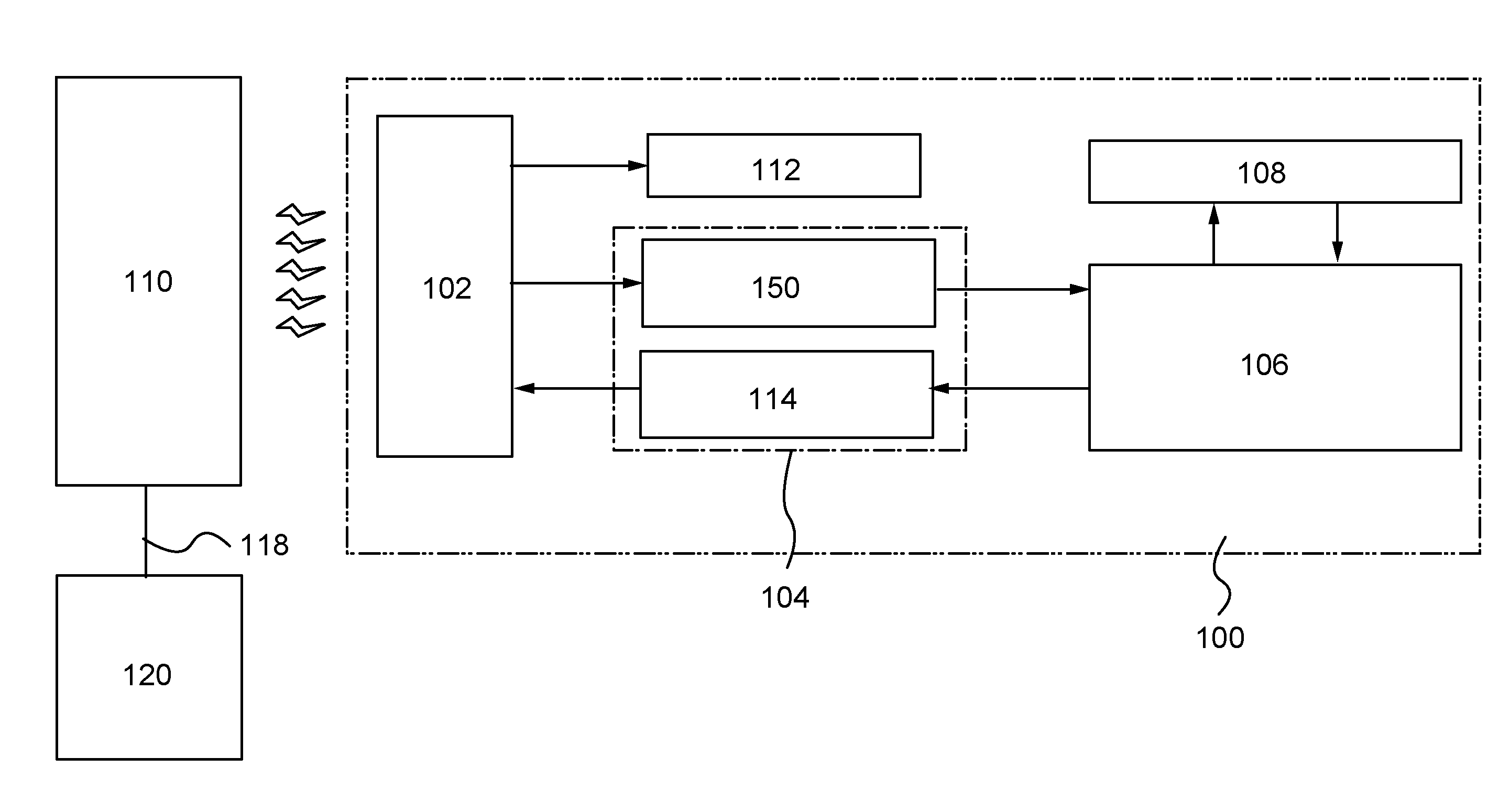
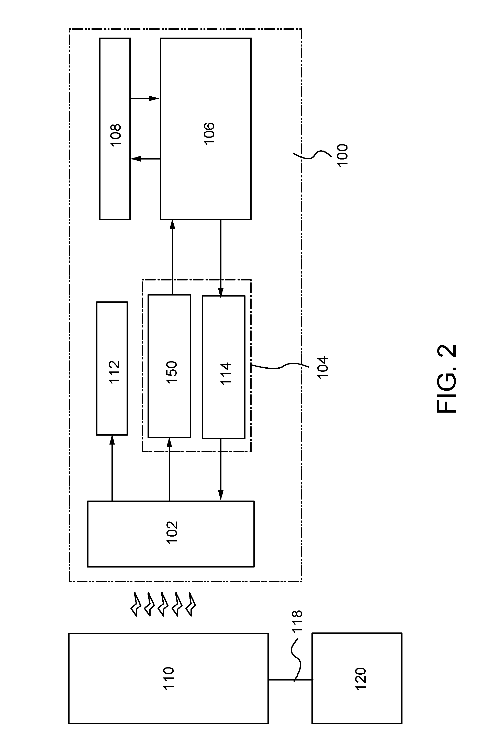
[0049]FIG. 2 illustrates a block diagram of a semiconductor device according to an embodiment of the present invention. A semiconductor device 100 according to an embodiment of the present invention transmits and receives data wirelessly to and from a reader / writer 110 by an electromagnetic wave. The reader / writer 110 is preferably connected to a control device 120 through a communication line 118. The control device 120 controls communication between the reader / writer 110 and the semiconductor device 100.

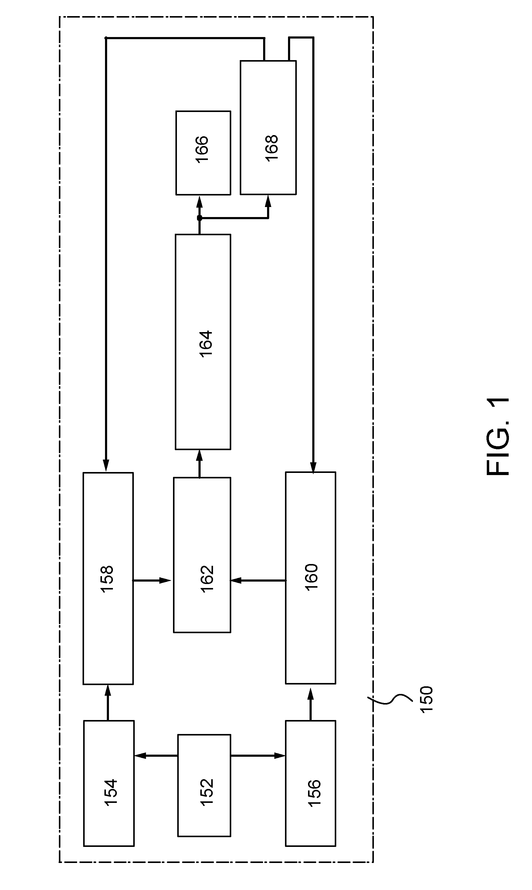
[0050]The semiconductor device 100 includes an antenna circuit 102, a power supply circuit 112, an analog circuit 104, a digital circuit 106 (including a control circuit), and a memory circuit 108. The analog circuit 104 has a demodulation signal gene...

embodiment 2

[0098]In one mode of this embodiment, an example of a manufacturing method of the semiconductor device described in Embodiment 1 will be described with reference to drawings. In one mode of this embodiment, a structure of the semiconductor device in which an antenna, a battery, and a signal processing circuit are formed over one substrate using a thin film transistor will be described. Note that miniaturization can be achieved by formation of an antenna, a battery, and a signal processing circuit over one substrate. Further, an example in which a thin film secondary battery is used as the battery will be described.

[0099]First, a separation layer 3403 is formed over one surface of a substrate 3401 with an insulating film 3402 interposed therebetween, and then an insulating film 3404 which functions as a base film and an amorphous semiconductor film 3405 (e.g., a film containing amorphous silicon) are stacked thereover (see FIG. 10A). Note that the insulating film 3402, the separation...

embodiment 3

[0154]In one mode of this embodiment, an example of the method for manufacturing the semiconductor device, which is described in one mode of the above embodiment, will be described with reference to drawings. In one mode of this embodiment, a structure in which an antenna, a battery, and a signal processing circuit of the semiconductor device are formed over one substrate will be described. Note that an antenna, a battery, and a signal processing circuit are formed together over a single crystal substrate, using a transistor including a channel formation region. When a transistor is formed over a single crystal substrate, a semiconductor device having a transistor with few variations in electric characteristics can be formed, which is preferable. In addition, an example is described in which a thin-film secondary battery is used as a battery.

[0155]First, a region 3504 and a region 3506 are formed in a semiconductor substrate 3500 by separating an element region (see FIG. 15A). The r...


PUM


Abstract

A semiconductor device is provided, which comprises a first demodulation circuit, a second demodulation circuit, a first bias circuit, a second bias circuit, a comparator, an analog buffer circuit, and a pulse detection circuit. An input portion of the pulse detection circuit is electrically connected to an output portion of the analog buffer circuit, a first output portion of the pulse detection circuit is electrically connected to an input portion of the first bias circuit, and a second output portion of the pulse detection circuit is electrically connected to an input portion of the second bias circuit.

Description

BACKGROUND OF THE INVENTION[0001]1. Field of the Invention[0002]The present invention relates to a semiconductor device. In particular, the present invention relates to a semiconductor device capable of transmitting and receiving information without contact by utilizing wireless communication.[0003]2. Description of the Related Art[0004]In recent years, individual recognition technology in which individual identification information is given to an individual object to clarify information such as a history of the object has attracted attention. In particular, the development of semiconductor devices capable of transmitting and receiving data without contact by wireless communication through a radio wave has been advanced. Such semiconductor devices are referred to as an IC tag, an RFID tag, and the like, which have begun to be used for management of articles in markets, or the like.[0005]In general, many of objects which are referred to as an RFID tag and the like that have been put ...

Claims


Application Information

Patent Timeline
IPC IPC(8): H04L27/06G06K19/07G06K19/077H01L21/822H01L21/8234H01L27/04H01L27/06H01L27/08H01L27/088H03D1/10H03D1/18
CPCH04L27/06G06K19/07749H04B1/40H04L27/38
Inventor MATSUZAKI, TAKANORI
Owner SEMICON ENERGY LAB CO LTD
Why Eureka
Try Eureka