

Method for repairing elecrical circuit of circuit board
- Summary
- Abstract
- Description
- Claims
- Application Information
AI Technical Summary
Benefits of technology
Problems solved by technology
Method used
Image

Examples
first preferred embodiment
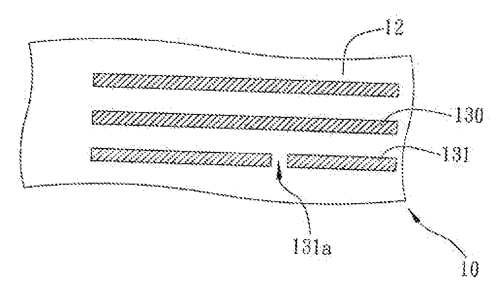
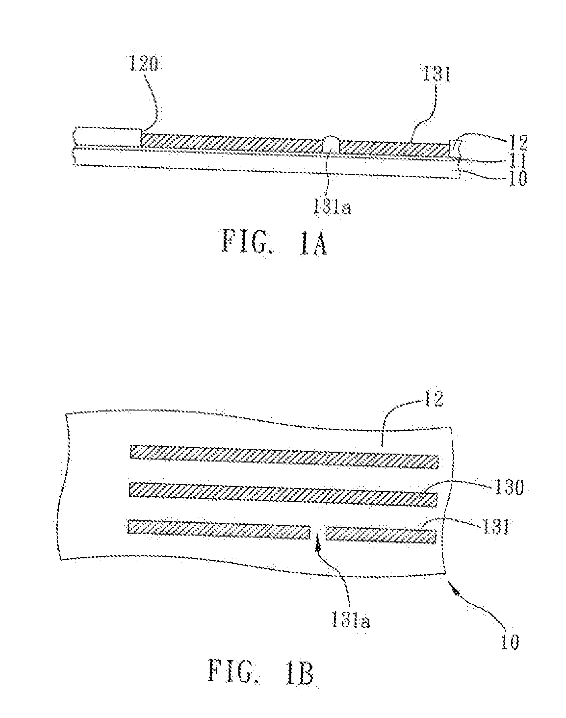
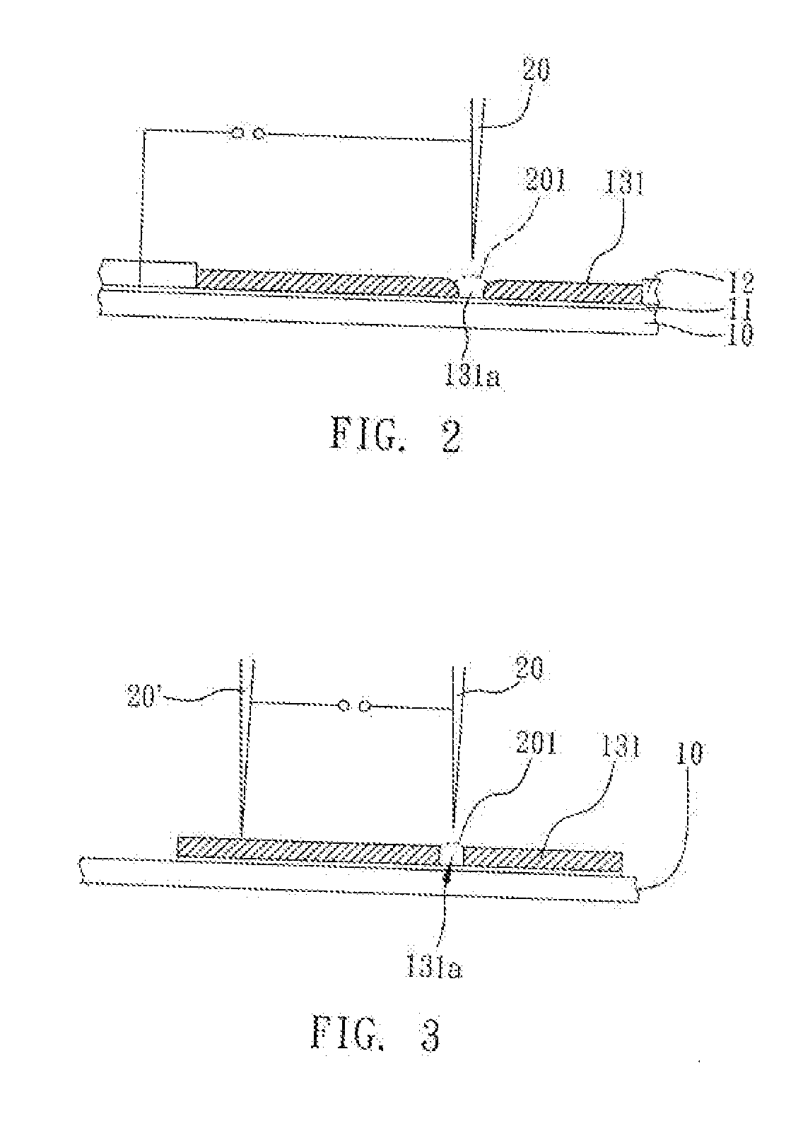
[0027]FIGS. 1A to 1B are a cross-sectional view and a top view of a structure of a circuit board according to the present invention, and FIG. 2 is illustrative a cross-sectional view representing a method for repairing a circuit defect of a circuit board according to a first preferred embodiment of the present invention.
[0028]Referring to FIG. 1A, first of all, a circuit board 10 is provided, a conductive layer 11 is formed on at least one surface of the circuit board 10, and a resist layer 12 is formed on the conductive layer 11, wherein the resist layer 12 has a plurality of openings 120 formed therein to expose a portion of the conductive layer 11, so as to form a patterned circuit layer having a plurality of electrical circuits 130 and 131 on the exposed area of the conductive layer 11 by an electroplating process, and there is a defect in the electrical circuit 131, wherein a portion of the electrical circuit 131 is deficient. In this embodiment, the defect in the electrical ci...
second preferred embodiment
[0030]FIG. 3 is illustrative a cross-sectional view representing a method for repairing a circuit defect of a circuit board according to a second preferred embodiment of the present invention. In this embodiment, different from the first embodiment, the micro-electroplating process is performed after a step of removing the resist layer and the conductive layer covered by the resist layer, that is to say, the electrical circuit layer of the circuit board is entirely exposed by removing the resist layer and the conductive layer, and the microelectrode 20 functions as an oxidizing terminal of electroplating, the electrical circuit 131 of the circuit board 10 contacting another microelectrode 20′ functions as a reducing terminal of electroplating, so as to generate a current path for performing a micro-electroplating process, and the microelectrode 20 is used to plate the circuit material on the area where the open circuit defect 131a occurred in the electrical circuit 131, thereby an e...
third preferred embodiment
[0031]FIGS. 4A to 4B are illustrative cross-sectional views representing a method for repairing a circuit defect of a circuit board according to a third preferred embodiment of the present invention. In this embodiment, different from the first embodiment, micro-droplet is used to repair the electrical circuit in which the defect occurred, and the steps for the repairing process will be described in detail as follows.
[0032]Referring to FIG. 4A, a conductive layer is formed on at least one surface of the circuit board 10, and a resist layer is formed on the conductive layer 11, wherein the resist layer has a plurality of opening formed therein to expose the conductive layer, so as to form a patterned circuit layer on the exposed area of the conductive layer by an electroplating process, and the electrical layer having an electrical circuit 131 in which an open circuit defect 131a occurred. The micro-droplet 30 is supplied for performing an micro-deposition process, so as to deposit t...
PUM
 Abstract
Description
Claims
Application Information