Package module of light emitting diode

a technology of light-emitting diodes and packaging modules, which is applied in the direction of basic electric elements, electrical apparatus, semiconductor devices, etc., can solve the problems of high cost of packaging devices one by one and waste, and achieve the effect of eliminating additional photosensors and reducing the cost of packaging processes

Inactive Publication Date: 2007-12-06
GIGNO TECH CO LTD
View PDF9 Cites 41 Cited by
  • Summary
  • Abstract
  • Description
  • Claims
  • Application Information

AI Technical Summary

Benefits of technology

[0010]In view of the foregoing, the invention is to provide a package module of a light emitting diode, in which the light emitting diode and a transistor may be packaged in the same package so that the cost of the packaging process may be reduced.
[0011]In addition, the invention is to provide a package module of a light emitting diode, in which any two of the light emitting diode, a transistor and a photosensor may be packaged in the same package so that the cost of the packaging process may be reduced.
[0014]As mentioned above, the first LED and the transistor are disposed on the substrate, and the first LED and the transistor are disposed in the same package in the package module of the LED according to the invention. Compared with the prior art, the cost of the packaging process may be reduced by disposing the first LED and the transistor in the same package. In addition, when the second LED is driven by the reverse bias in the embodiment of the invention, the photosensor for sensing the light emitting intensity is formed. Thus, the intensity of the LED may be adjusted according to the feedback, and it is possible to eliminate the additional photosensor for sensing the light intensity.

Problems solved by technology

Consequently, the cost of packaging the devices one by one becomes high and is thus wasted.

Method used


Image

  • Package module of light emitting diode
  • Package module of light emitting diode
  • Package module of light emitting diode

Examples


Embodiment Construction

[0028]The present invention will be apparent from the following detailed description, which proceeds with reference to the accompanying drawings, wherein the same references relate to the same elements.

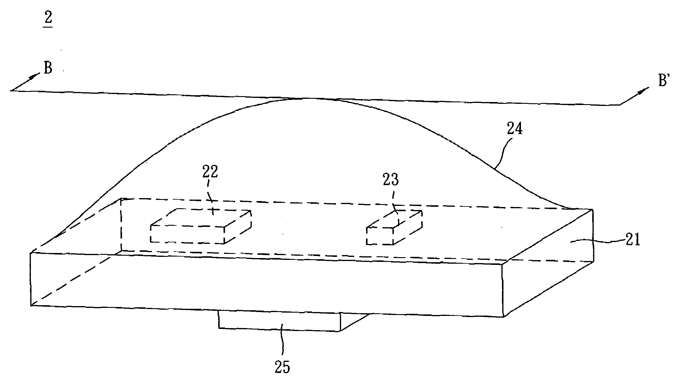
[0029]Referring to FIGS. 3 and 4, a package module 2 of a light emitting diode (LED) according to this embodiment of the invention includes a substrate 21, a first LED 22 and a transistor 23, wherein the first LED 22 and the transistor 23 are disposed in the same package 24.

[0030]In this embodiment, the substrate 21 is not particularly restricted and may be a printed circuit board, a heat dissipating plate or a glass substrate. The material of the package 24 is not particularly restricted and may be a transparent resin, such as a transparent epoxy resin, or a transparent glue, such as silicone.

[0031]As shown in FIG. 4, the first LED 22 of this embodiment may be a LED chip or a LED die (bare chip or die) directly disposed on the substrate 21.

[0032]The transistor 23, which is electrical...


PUM


Abstract

A package module of a light emitting diode includes a substrate, a first light emitting diode and a transistor. The first light emitting diode is disposed on the substrate, and the transistor is electrically connected with the first light emitting diode. The transistor is disposed on the substrate and turns on or off the first light emitting diode. The first light emitting diode and the transistor are disposed in a same package.

Description

CROSS REFERENCE TO RELATED APPLICATIONS[0001]This Non-provisional application claims priority under 35 U.S.C. §119(a) on Patent Application No(s). 095114747 filed in Taiwan, Republic of China on Apr. 25, 2006, the entire contents of which are hereby incorporated by reference.BACKGROUND OF THE INVENTION[0002]1. Field of Invention[0003]The invention relates to a package module of a diode, and, in particular, to a package module of a light emitting diode.[0004]2. Related Art[0005]With the high development of the technology, light emitting diodes (LEDs) having the advantages of the lightness, the power-saving property and the long lifetime have been currently and widely applied to indicators and displays of information, communication and consumer electronic products, such as an indicator lamp, a portable flashlight, a liquid crystal display (LCD) backlight plate, a floor lamp, an emergency lamp, a medical apparatus light source, auxiliary illumination, main illumination, and the like. S...

Claims


Application Information

Patent Timeline
Patent Type & Authority Applications(United States)
IPC IPC(8): H01L33/00H01L31/12
CPCH01L25/167H01L31/0203H01L2924/0002H01L2924/00
Inventor LIN, FENG-LI
Owner GIGNO TECH CO LTD
Why Eureka
Try Eureka