Organic electroluminescence device and organic electroluminescence panel using the same

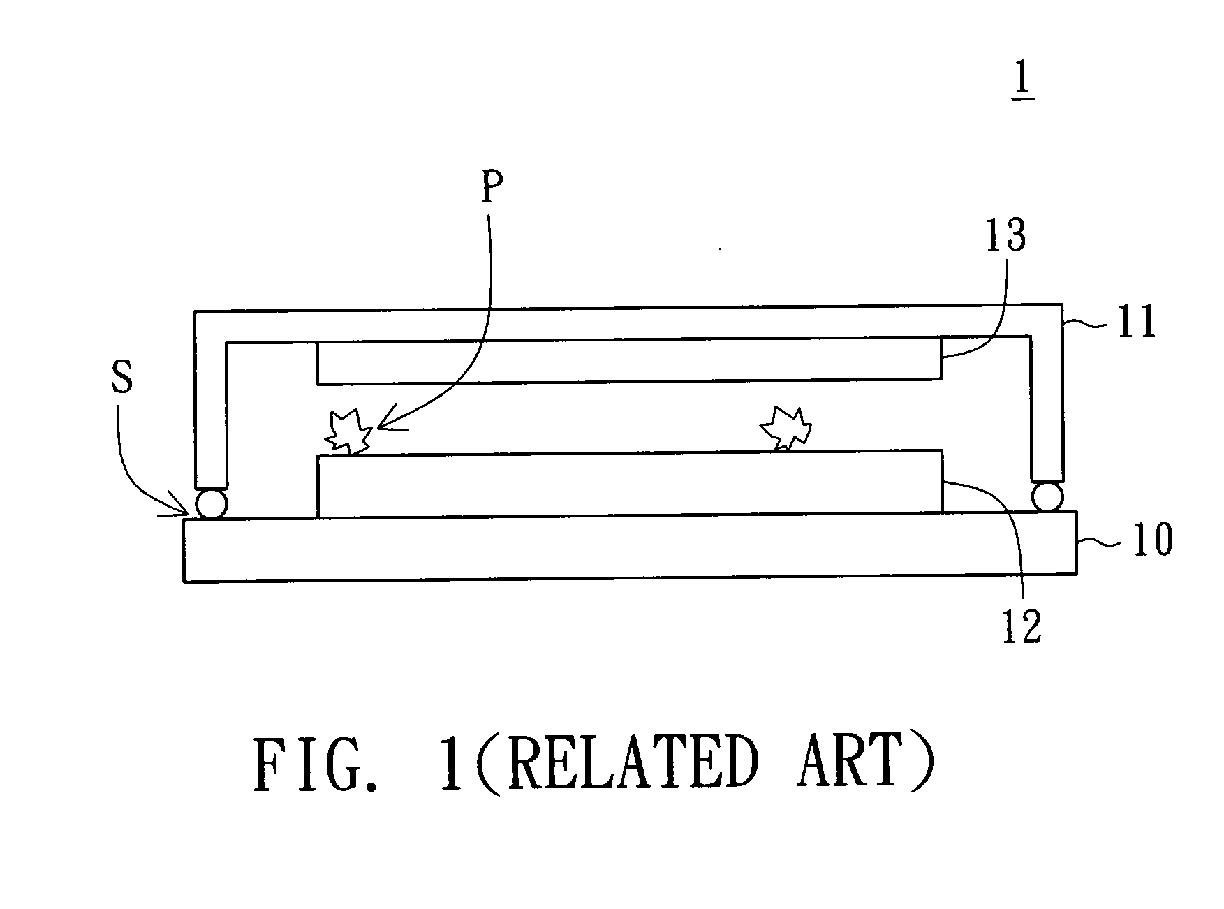
a technology of organic electroluminescence and electroluminescence panel, which is applied in the direction of discharge tube luminescnet screen, discharge tube/lamp details, electric discharge lamps, etc., can solve the problems of easy pressed and damaged oeld b>12/b>, affecting the yield rate and reliability of the product,

Active Publication Date: 2007-12-06
AU OPTRONICS CORP
View PDF12 Cites 14 Cited by
  • Summary
  • Abstract
  • Description
  • Claims
  • Application Information

AI Technical Summary

Benefits of technology

[0008]It is therefore an object of the invention to provide an organic electroluminescence device (OELD) and an OEL panel using the same. A shielding structure is formed on the electrode of the OELD. The hardness of the shielding structure is smaller than the hardness of the electrode.

Problems solved by technology

Due to the fragile structure of the OELD 12, if the top cover 11 or the substrate 10 is bent or deformed during the packaging process or back-end process of the OEL panel 1, the OELD 12 would easily be pressed and damaged.
Due to the structure design and physical characteristics of the OEL panel, if particle problem occurs to the display panel, the illuminant element would be pressed and damaged easily, affecting the yield rate and reliability of the product.

Method used


Image

  • Organic electroluminescence device and organic electroluminescence panel using the same
  • Organic electroluminescence device and organic electroluminescence panel using the same
  • Organic electroluminescence device and organic electroluminescence panel using the same

Examples


first embodiment

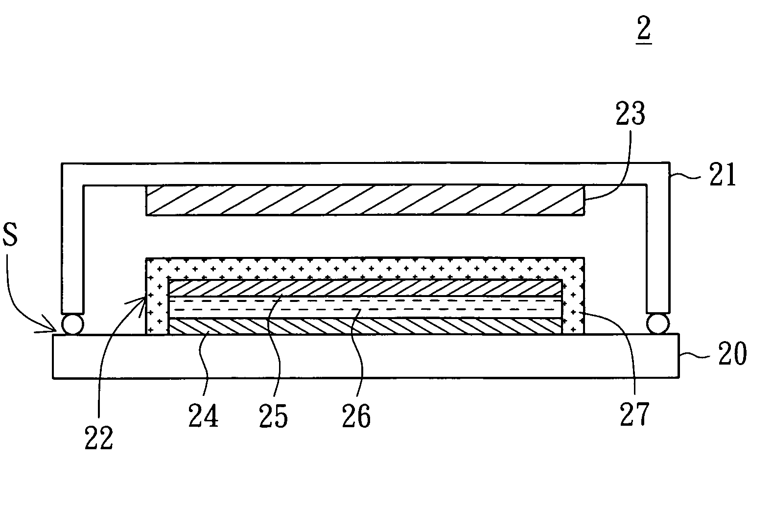
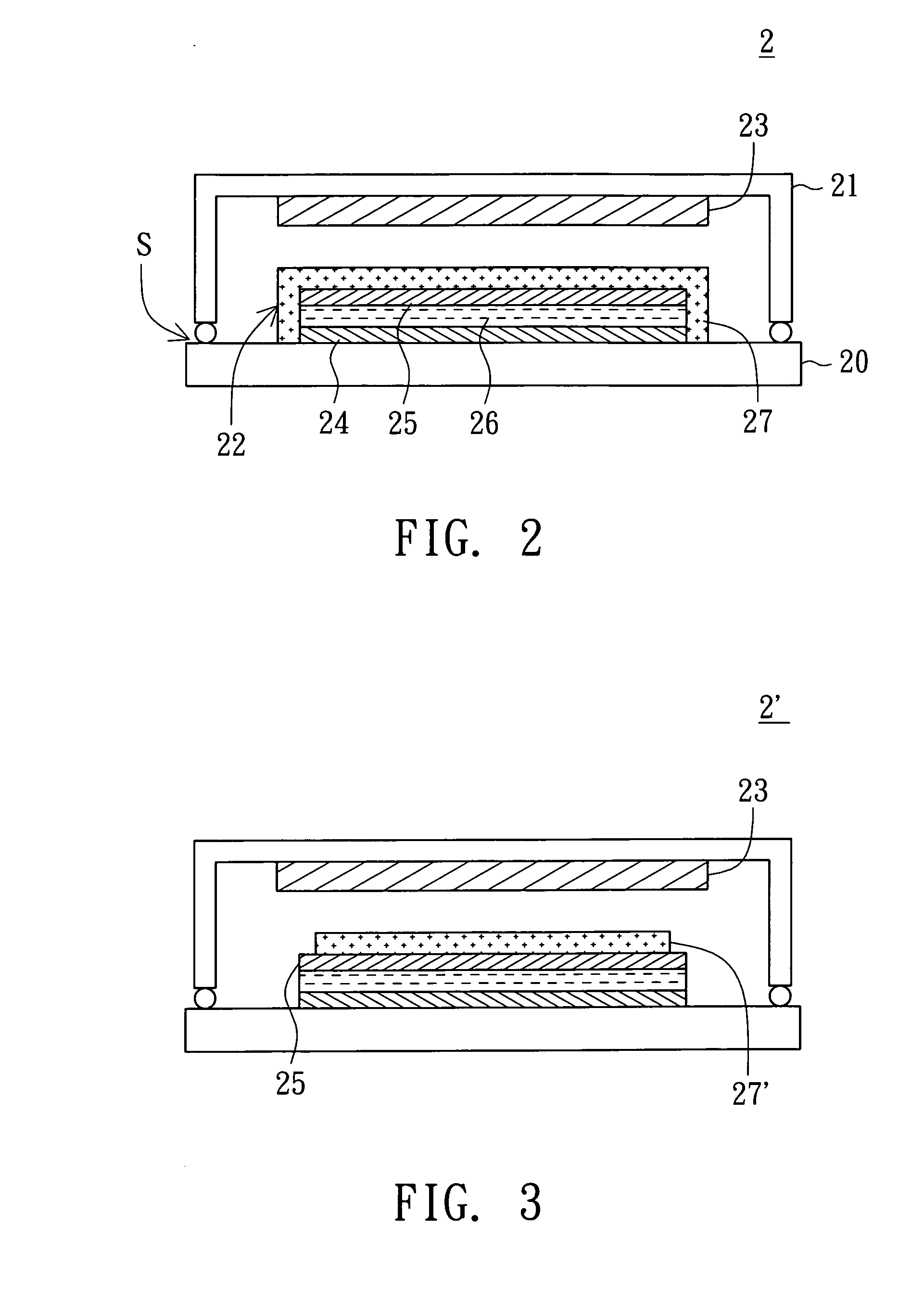
[0017]Referring to FIG. 2, a first diagram of an OEL panel according to a first embodiment of the invention is shown. As shown in FIG. 2, the OEL panel 2 mainly comprises a substrate 20, a top cover 21 and an OELD 22. The top cover 21 is disposed on the substrate 20. The OELD 22 is disposed on the substrate 20 and positioned between the top cover 21 and the substrate 20. The OELD 22 comprises a first electrode 24, a second electrode 25, an emissive layer 26 and a shielding structure 27. The second electrode 25 is disposed above the first electrode 24. The emissive layer 26 is disposed between the first electrode 24 and the second electrode 25. The shielding structure 27 is disposed on the second electrode 25 as a buffer layer in order to protect the OELD from being scratched or damaged by particles. The hardness of the shielding structure 27 is smaller than the hardness of the second electrode 25. The yield rate of the OEL panel can be improved.

[0018]A sealant S is filled between th...

second embodiment

[0027]Referring to FIG. 4, a first diagram of an OEL panel according to a second embodiment of the invention is shown. The OEL panel 3 of the present embodiment of the invention differs with the OEL panel 2 of the first embodiment in the elements of the OELD. As for other similar elements, the same reference numbers are used and are not repeated here. As shown in FIG. 4, the OELD 32 of the OEL panel 3 comprises a first electrode 34, a second electrode 35, an emissive layer 36 and a shielding structure 37. The emissive layer 36 is disposed between the first electrode 34 and the second electrode 35. The shielding structure 37 is disposed on the second electrode 35. The hardness of the shielding structure 37 is approximately smaller than or equal to the hardness of the second electrode 35.

[0028]In practical application, the shielding structure 37 may comprise several shielding layers, wherein the present embodiment of the invention is exemplified by having two shielding layers. In FIG....


PUM


Abstract

An organic electroluminescence device (OELD) and a display panel are provided. The OELD comprises a first electrode, a second electrode, an emissive layer and a shielding structure. The second electrode is disposed above the first electrode. The emissive layer is disposed between the first electrode and the second electrode. The shielding structure is disposed above the second electrode. The hardness of the shielding structure is smaller than that of the second electrode.

Description

[0001]This application claims the benefit of Taiwan Patent Application Serial No. 95119834, filed Jun. 5, 2006, the subject matter of which is incorporated herein by reference.BACKGROUND OF THE INVENTION[0002]1. Field of the Invention[0003]The invention relates in general to an organic electroluminescence device (OELD) and an organic electroluminescence (OEL) panel using the same, and more particularly to an OELD having a shielding structure on the electrode and an OEL panel using the same. The hardness of the shielding structure is approximately smaller than or equal to the hardness of the electrode.[0004]2. Description of the Related Art[0005]The OEL panel having the advantages of light weight, thinness, high contrast, power saving, high color saturation, and fast response has become a display with great potential. Both the manufacturing process and the structure of an organic electroluminescence device (OELD) are simpler than that of other display devices such as cathode ray tube...

Claims


Application Information

Patent Timeline
Patent Type & Authority Applications(United States)
IPC IPC(8): H05B33/02
CPCH01L51/5237H10K50/8423H10K50/846H10K50/844
Inventor HU, MIN-CHIEHHUNG, MIN-LING
Owner AU OPTRONICS CORP
Why Eureka
Try Eureka