Order selected overlay metrology

a metrology and overlay technology, applied in the field of order selected overlay metrology, can solve the problems of affecting the alignment or offset of the structure of one layer or pattern, and achieve the effect of avoiding the offset or misalignment of the structur

Active Publication Date: 2007-12-06
KLA TENCOR TECH CORP
View PDF6 Cites 63 Cited by
  • Summary
  • Abstract
  • Description
  • Claims
  • Application Information

AI Technical Summary

Benefits of technology

[0013] In another embodiment, the invention pertains to at least one computer readable storage medium having computer program instructions stored thereon that are arranged to perform one or more of the above described o

Problems solved by technology

If the two layers or patterns are not properly formed, then the structure on one layer or pat

Method used


Image

  • Order selected overlay metrology
  • Order selected overlay metrology
  • Order selected overlay metrology

Examples


Embodiment Construction

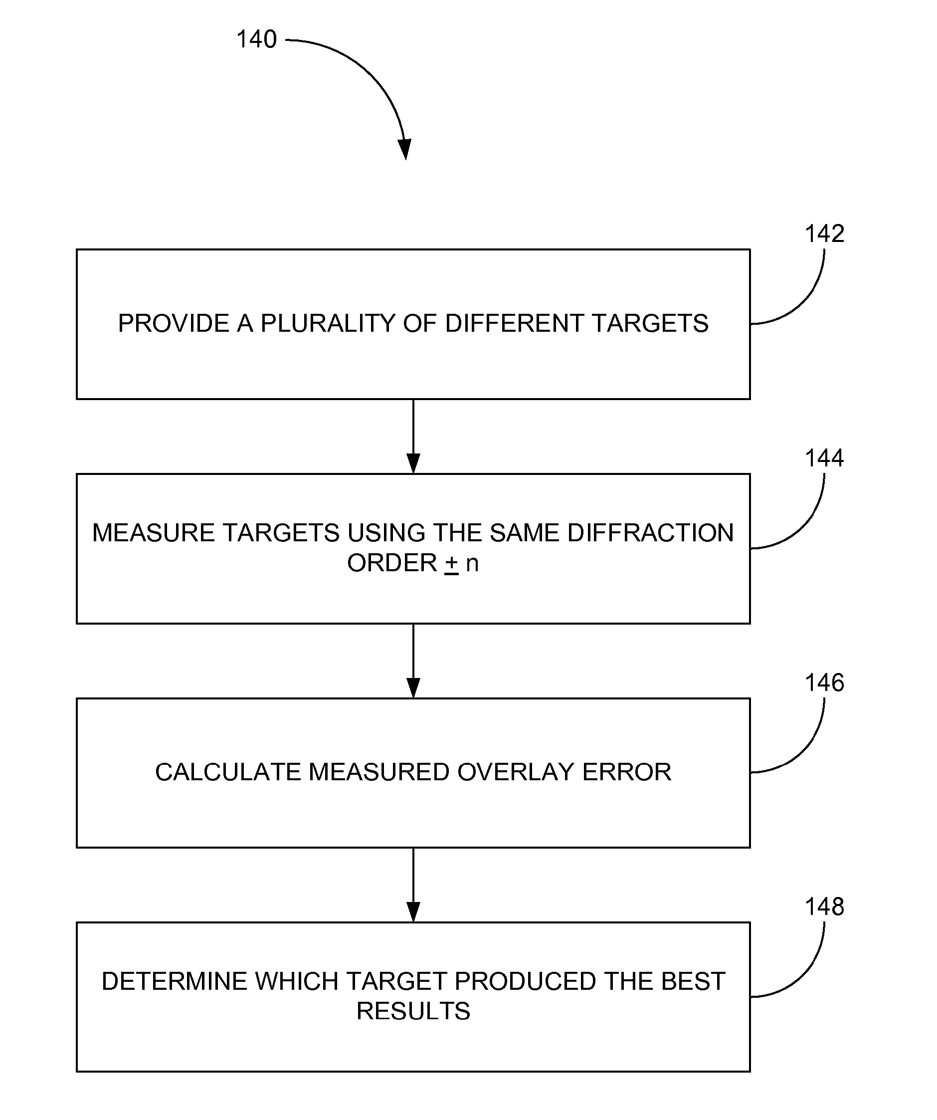
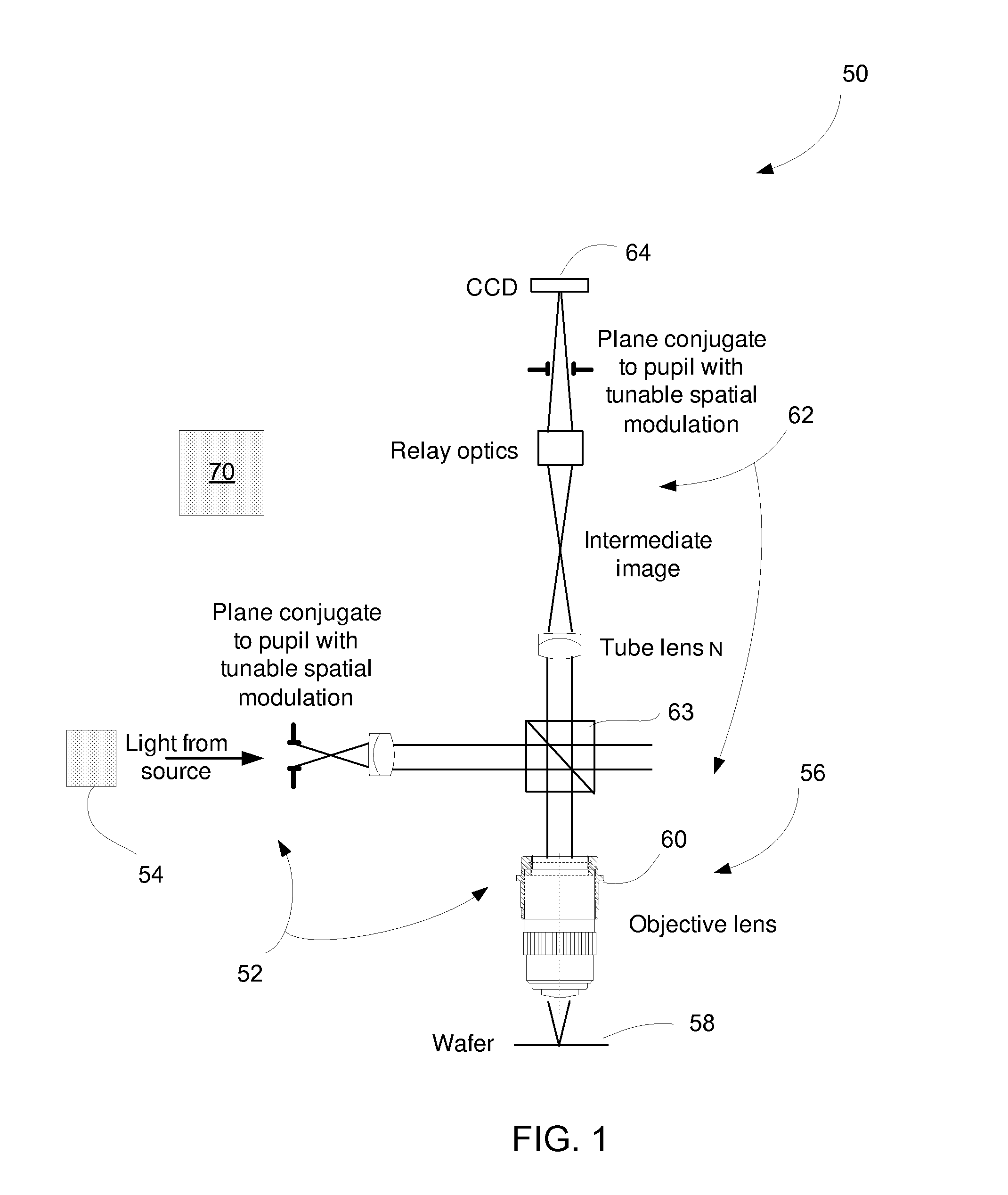
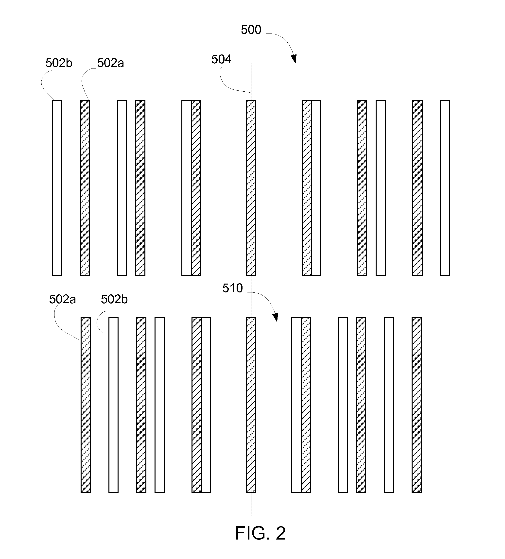
[0032] Reference will now be made in detail to a specific embodiment of the invention. An example of this embodiment is illustrated in the accompanying drawings. While the invention will be described in conjunction with this specific embodiment, it will be understood that it is not intended to limit the invention to one embodiment. On the contrary, it is intended to cover alternatives, modifications, and equivalents as may be included within the spirit and scope of the invention as defined by the appended claims. In the following description, numerous specific details are set forth in order to provide a thorough understanding of the present invention. The present invention may be practiced without some or all of these specific details. In other instances, well known process operations have not been described in detail in order not to unnecessarily obscure the present invention.

[0033] In general, embodiments of the invention pertain to systems and methods are described herein with r...


PUM


Abstract

Disclosed are apparatus and methods for measuring a characteristic, such as overlay, of a semiconductor target. In general, order-selected imaging and/or illumination is performed while collecting an image from a target using a metrology system. In one implementation, tunable spatial modulation is provided only in the imaging path of the system. In other implementations, tunable spatial modulation is provided in both the illumination and imaging paths of the system. In a specific implementation, tunable spatial modulation is used to image side-by-side gratings with diffraction orders ±n. The side-by-side gratings may be in different layers or the same layer of a semiconductor wafer. The overlay between the structures is typically found by measuring the distance between centers symmetry of the gratings. In this embodiment, only orders ±n for a given choice of n (where n is an integer and not equal to zero) are selected, and the gratings are only imaged with these diffraction orders.

Description

CROSS REFERENCE TO RELATED APPLICATIONS [0001] The present application claims priority under 35 U.S.C. § 119(e) from U.S. Provisional Patent Application No. 60 / 810,560 entitled “ORDER SELECTED OVERLAY METROLOGY” filed Jun. 1, 2006 (Attorney Docket No. KLA1P172P / P1883 / PRO), and U.S. Provisional Patent Application No. 60 / 897,637 entitled “SYSTEMS AND TECHNIQUES FOR SEMICONDUCTOR METROLOGY INSPECTION” filed Jan. 26, 2007 (Attorney Docket No. KLA1P178P2), which applications are incorporated herein by reference for all purposes.BACKGROUND OF THE INVENTION [0002] The invention pertains to systems and methods for performing overlay measurements on semiconductor structures and the like. [0003] An overlay measurement generally specifies how accurately a first patterned layer aligns with respect to a second patterned layer disposed above or below it or how accurately a first pattern aligns with respect to a second pattern disposed on the same layer. The overlay error is typically determined w...

Claims


Application Information

Patent Timeline
IPC IPC(8): G01B11/00
CPCG03F7/70633
Inventor KANDEL, DANIELLEVINSKI, VLADIMIRADEL, MICHAEL E.SELIGSON, JOEL L.
Owner KLA TENCOR TECH CORP
Why Eureka
Try Eureka